 ChipApex | Global Electronic Components Supplier
SEARCH
Search Product
Search Post
— IC芯片 | 连接器 | 传感器 | 被动器件 —
Search productSearch post
— IC芯片 | 连接器 | 传感器 | 被动器件 —
Consult the customer manager about the wholesale price.
consultation hotline:86-132-6715-2157
email:[email protected]
Contact the product manager for consultation. One-stop consultation is available.
Do you want a lower wholesale price? Please send us your inquiry and we will reply immediately.
The PDTA113ZE,115 is a PNP resistor-equipped transistor (RET) manufactured by NXP Semiconductors. It integrates a single PNP transistor with built-in bias resistors R1 and R2 in an SOT416 (SC-75) surface-mounted plastic package. The device features a collector-emitter voltage of -50 V and a DC output current capability of -100 mA. Internal resistance values are specified as R1 = 1 kΩ and R2 = 10 kΩ, with a typical ratio of 10. This integration simplifies circuit design by reducing component count and pick-and-place costs while maintaining high temperature operation up to 150 °C junction temperature.
Verify the specific ordering suffix against the manufacturer's official documentation to confirm the exact package variant and packing method. Ensure compatibility with the required surface mount technology processes. Confirm that the thermal characteristics align with the intended ambient operating conditions and power dissipation limits defined in the product data sheet.
Select this component when a compact solution for driving logic inputs or interfacing digital signals is required. The integrated bias network eliminates the need for external base resistors, streamlining the schematic. Consider the SOT416 package dimensions for layout constraints. Verify that the -50 V rating and -100 mA current limit meet the specific load requirements of the application circuit.
The PDTA113ZE belongs to the PDTA113Z series of PNP resistor-equipped transistors. It serves as the PNP counterpart to the PDTC113ZE NPN RET. The series offers multiple package options including SOT23, SOT323, and SOT883, allowing designers to choose form factors based on space and mounting preferences while maintaining consistent electrical performance characteristics across the family.
Direct functional substitutes within the same series include PDTA113ZK, PDTA113ZM, PDTA113ZS, PDTA113ZT, and PDTA113ZU. These variants share identical electrical specifications but differ in physical package geometry. Ensure the replacement package matches the PCB footprint and soldering process capabilities.
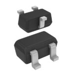 PDTA113ZE,115
The activity of extra discounts on wholesale prices is in full swing…
Please fill in your contact information and we will send you the latest wholesale price list.





