 ChipApex | Global Electronic Components Supplier
SEARCH
Search Product
Search Post
— IC芯片 | 连接器 | 传感器 | 被动器件 —
Search productSearch post
— IC芯片 | 连接器 | 传感器 | 被动器件 —
Consult the customer manager about the wholesale price.
consultation hotline:86-132-6715-2157
email:[email protected]
Contact the product manager for consultation. One-stop consultation is available.
Do you want a lower wholesale price? Please send us your inquiry and we will reply immediately.
The PDTA144EQBZ is a PNP Resistor-Equipped Transistor (RET) from the Nexperia PDTA143/114/124/144EQB series. It features built-in bias resistors R1 and R2, both nominally 47 kΩ. The device operates with a collector-emitter voltage of -50 V and an output current capability of 100 mA. It is housed in an ultra-small DFN1110D-3 (SOT8015) leadless package measuring 1.1 x 1.0 x 0.48 mm with side-wettable flanks. Key electrical characteristics include a DC current gain (hFE) of 80 at -5 mA and a transition frequency of 180 MHz.
Verify the specific ordering code against the manufacturer's official database to ensure correct package variant and marking code. Confirm that the DFN1110D-3 footprint matches the target PCB layout requirements. Check for any recent product status updates or lifecycle notices directly from the supplier before finalizing procurement plans.
Select this component when a compact PNP switching solution with integrated base biasing is required. The 47 kΩ resistor values are suitable for standard digital interface driving. Ensure the application voltage does not exceed the -50 V collector-emitter rating and that thermal dissipation remains within the specified junction temperature limits.
This part belongs to the PDTA14x EQB series, which shares the same SOT8015 package but varies in internal resistor values. Complementary NPN versions are available as PDTC143EQB through PDTC144EQB. The series is designed as a cost-saving alternative to discrete transistor and resistor combinations in digital circuits.
Direct substitutes include other PNP RETs with similar 47 kΩ bias resistors and compatible pinouts. Verify package dimensions and thermal resistance if replacing with components from different manufacturers. Ensure the replacement supports the required -50 V breakdown voltage and 100 mA current handling.
Both R1 (input/base) and R2 (emitter/GND) have nominal values of 47 kΩ.
The DFN1110D-3 package features side-wettable flanks, allowing for Automatic Optical Inspection (AOI) of the solder joints.
The maximum collector-emitter voltage (VCEO) is -50 V.
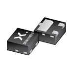 PDTA144EQBZ
The activity of extra discounts on wholesale prices is in full swing…
Please fill in your contact information and we will send you the latest wholesale price list.





