 ChipApex | Global Electronic Components Supplier
SEARCH
Search Product
Search Post
— IC芯片 | 连接器 | 传感器 | 被动器件 —
Search productSearch post
— IC芯片 | 连接器 | 传感器 | 被动器件 —
Consult the customer manager about the wholesale price.
consultation hotline:86-132-6715-2157
email:[email protected]
Contact the product manager for consultation. One-stop consultation is available.
Do you want a lower wholesale price? Please send us your inquiry and we will reply immediately.
The PDTB123TK is a PNP Resistor-Equipped Transistor (RET) from the NXP PDTB123T series, housed in an SOT346 (SC-59A) surface-mount package. It integrates a single bias resistor with a value of 2.2 kΩ, while the second resistor position remains open. The device supports a maximum collector-emitter voltage of -50 V and provides a continuous DC output current capability of -500 mA. Key electrical characteristics include a typical DC current gain (hFE) of 250 at -50 mA and a maximum collector-emitter saturation voltage of -0.3 V under specified test conditions.
Verify the specific ordering suffix against the manufacturer's official documentation to confirm the exact packing method and reel specifications. Confirm that the SOT346 package variant matches the required footprint dimensions and pin alignment for the target PCB layout before finalizing procurement orders.
Select this component when a PNP switching solution with integrated base biasing is required. Ensure the application voltage does not exceed the -50 V collector-emitter rating and that the load current remains within the -500 mA limit. Verify thermal dissipation requirements against the junction-to-ambient resistance values provided in the datasheet.
This part belongs to the PDTB123T family of PNP resistor-equipped transistors. It serves as the PNP counterpart to the NPN PDTD123TK model. The series is designed to replace standard BC807 series transistors in digital applications by providing pre-biased functionality in a compact surface-mount form factor.
The NXP PDTD123TK is the documented NPN complement within the same product family. Other variants in the series include PDTB123TS and PDTB123TT, which utilize different package types such as SOT54 and SOT23 respectively.
The PDTB123TK features one built-in bias resistor (R1) with a nominal value of 2.2 kΩ connected to the input. The second resistor position (R2) is left open.
The marking code printed on the PDTB123TK device is 'F1'.
For the SOT346 package, Pin 1 is the input (base), Pin 2 is GND (emitter), and Pin 3 is the output (collector).
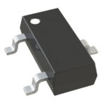 PDTB123TK,115
The activity of extra discounts on wholesale prices is in full swing…
Please fill in your contact information and we will send you the latest wholesale price list.






