ChipApex | Global Electronic Components Supplier

SEARCH
Search Product
Search Post
— IC芯片 | 连接器 | 传感器 | 被动器件 —
Search productSearch post
— IC芯片 | 连接器 | 传感器 | 被动器件 —
Consult the customer manager about the wholesale price.
consultation hotline:86-132-6715-2157
email:[email protected]
Contact the product manager for consultation. One-stop consultation is available.
Do you want a lower wholesale price? Please send us your inquiry and we will reply immediately.
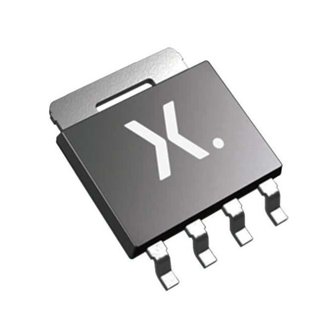
PH3230S,115 is listed in the Single FETs, MOSFETs range at ChipApex. The manufacturer field lists Nexperia USA Inc.. Its product description is MOSFET N-CH 30V 100A LFPAK. Review the specifications below when checking this part for your BOM.
The PH3230S is an N-channel TrenchMOS intermediate level Field-Effect Transistor (FET) housed in a plastic LFPAK (SOT669) package. It features a drain-source voltage rating of 30 V and a continuous drain current capability of 100 A at 25 °C mounting base temperature. The device exhibits a maximum on-state resistance of 3.2 mΩ at VGS = 10 V and 56.5 mΩ at VGS = 4.5 V, both measured at ID = 25 A and Tj = 25 °C. Total power dissipation reaches 62.5 W under specified thermal conditions.
Verify the specific ordering suffix and package variant against the manufacturer's current catalog before procurement. Confirm that the component status remains active for production use, as datasheet revisions may impact availability or specifications. Ensure compliance with export control regulations if applicable to your region. Cross-reference the pinning configuration with your PCB layout to guarantee correct source, gate, and drain connections.
Select this component for applications requiring high current handling within a compact surface-mount form factor. Evaluate the thermal resistance characteristics to ensure adequate heat sinking for the intended power dissipation levels. Consider the gate charge parameters when designing drive circuits to optimize switching speeds and minimize driver losses. Verify that the operating voltage and current limits remain within the safe operating area defined in the datasheet.
This N-channel enhancement mode FET utilizes TrenchMOS technology to achieve efficient performance in computing and communications equipment. Designed for industrial and consumer applications, it offers robust avalanche ruggedness with specified repetitive and non-repetitive energy ratings. The device integrates a source-drain diode with defined reverse recovery characteristics, supporting its use in synchronous rectification and inductive load switching scenarios.
No public substitute part numbers are documented in the provided datasheet.
The maximum peak drain current is 300 A for pulse durations less than or equal to 10 µs at a mounting base temperature of 25 °C.
Yes, the device includes a source-drain diode with a typical forward voltage of 0.8 V at 25 A and a reverse recovery time of 46 ns.
The thermal resistance from junction to mounting base is typically 2 K/W.
Explore related parts through FETs, MOSFETs, Transistors, Discrete Semiconductor Products, all product categories.
 PH3230S,115

The activity of extra discounts on wholesale prices is in full swing…
Please fill in your contact information and we will send you the latest wholesale price list.