 ChipApex | Global Electronic Components Supplier

SEARCH
Search Product
Search Post
— IC芯片 | 连接器 | 传感器 | 被动器件 —
Search productSearch post
— IC芯片 | 连接器 | 传感器 | 被动器件 —
Consult the customer manager about the wholesale price.
consultation hotline:86-132-6715-2157
email:[email protected]
Contact the product manager for consultation. One-stop consultation is available.
Do you want a lower wholesale price? Please send us your inquiry and we will reply immediately.
PI49FCT3807AQEX is listed in the Clock Buffers, Drivers range at ChipApex. The manufacturer field lists Diodes Incorporated. Its product description is IC CLK BUFFER 1:10 66MHZ 20QSOP. Review the specifications below when checking this part for your BOM.
The PI49FCT3807AQEX is a 3.3V Fast CMOS clock driver manufactured by Diodes Incorporated, featuring a 1-to-10 fanout configuration with one input and ten outputs. It operates within a supply voltage range of 3.0V to 3.6V and supports an industrial temperature range of –40°C to +85°C. The device provides ultra-low skew of 0.35ns typ and propagation delays between 1.5ns and 4.0ns max at CL=15pF. It accepts TTL-compatible inputs and drives CMOS outputs, ensuring low noise levels and minimal duty cycle distortion for clock distribution applications.
Verify the ordering suffix 'Q' corresponds to the 20-pin 150-mil wide QSOP package. Confirm the 'E' suffix indicates Pb-free and Green status. Ensure the 'X' suffix matches the required tape and reel packaging format. Check for RoHS3 compliance requirements against the datasheet specifications.
Select this component when a 1:10 non-inverting clock buffer is required with tight skew constraints. The QSOP package is suitable for space-constrained surface mount designs. Verify that the load capacitance does not exceed 15pF to maintain the specified maximum propagation delay of 4.0ns. Ensure the operating voltage remains within the 3.3V ±10% tolerance.
This part belongs to the PI49FCT series of 3.3V Fast CMOS logic circuits produced using advanced submicron technology. It is functionally equivalent to the legacy PI49FCT807 but optimized for 3.3V operation. The 'A' speed grade denotes specific timing characteristics distinct from B, C, or D grades available in the same family.
PI49FCT3807BQEX offers similar functionality with potentially different speed grade characteristics. PI49FCT3807DQEX provides alternative timing parameters within the same QSOP package. Cross-reference speed grades carefully as propagation delays vary between A, B, C, and D designations.
The maximum propagation delay is 4.0ns under test conditions of CL=15pF and RL=500Ω.
Yes, the device features 3-state Output Enable inputs (active LOW) allowing for clock busing applications.
The typical quiescent current (ICC) is 30µA at VCC = Max and VIN = GND or VCC.
Explore related parts through Clock/Timing, Integrated Circuits (ICs), all product categories, ChipApex homepage.
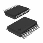 PI49FCT3807AQEX

The activity of extra discounts on wholesale prices is in full swing…
Please fill in your contact information and we will send you the latest wholesale price list.






