 ChipApex | Global Electronic Components Supplier

SEARCH
Search Product
Search Post
— IC芯片 | 连接器 | 传感器 | 被动器件 —
Search productSearch post
— IC芯片 | 连接器 | 传感器 | 被动器件 —
Consult the customer manager about the wholesale price.
consultation hotline:86-132-6715-2157
email:[email protected]
Contact the product manager for consultation. One-stop consultation is available.
Do you want a lower wholesale price? Please send us your inquiry and we will reply immediately.
PI49FCT805ATQE is listed in the Clock Buffers, Drivers range at ChipApex. The manufacturer field lists Diodes Incorporated. Its product description is IC CLK BUFFER 1:5 66MHZ 20QSOP. Review the specifications below when checking this part for your BOM.
The PI49FCT805ATQE is a non-inverting clock driver manufactured by Diodes Incorporated, housed in a 20-pin QSOP package. It comprises two independent driver banks, each providing five outputs from TTL-compatible CMOS inputs. The device features extremely low output skew of 0.5ns and includes a monitor output pin for performance verification. Electrical characteristics specify a maximum propagation delay of 5.8ns at CL=50pF. Operating voltage ranges from 4.75V to 5.25V, with an industrial temperature range of -40°C to +85°C.
Verify the 'A' speed grade suffix corresponds to the required 5.8ns maximum propagation delay specification. Confirm the 'Q' package code matches the 150-mil wide QSOP footprint requirements. Ensure the 'E' suffix indicates Pb-free and Green compliance if environmental standards are mandatory for the assembly process.
Select this component when low propagation delay and minimal skew are critical for timing alignment across multiple loads. The dual-bank design allows for separate clock domain management within a single package. Verify that the 50pF load capacitance requirement aligns with the target circuit design to ensure the specified switching characteristics are met.
This part belongs to the PI49FCT805 family of fast CMOS clock drivers. The 'A' suffix denotes a specific speed grade distinct from the standard, 'B', and 'C' variants found in the same series. It shares the same pinout and functional description as other speed grades but offers optimized switching performance parameters.
PI49FCT805TQE serves as a baseline replacement with different speed characteristics. PI49FCT805BTQE and PI49FCT805CTQE offer faster propagation delays. All variants maintain identical pin configurations and packaging.
Explore related parts through Clock/Timing, Integrated Circuits (ICs), all product categories, ChipApex homepage.
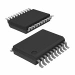 PI49FCT805ATQE

The activity of extra discounts on wholesale prices is in full swing…
Please fill in your contact information and we will send you the latest wholesale price list.






