 ChipApex | Global Electronic Components Supplier
SEARCH
Search Product
Search Post
— IC芯片 | 连接器 | 传感器 | 被动器件 —
Search productSearch post
— IC芯片 | 连接器 | 传感器 | 被动器件 —
Consult the customer manager about the wholesale price.
consultation hotline:86-132-6715-2157
email:[email protected]
Contact the product manager for consultation. One-stop consultation is available.
Do you want a lower wholesale price? Please send us your inquiry and we will reply immediately.
The PI6C20400BLEX is a PCIe 3.0 compliant high-speed, low-noise differential clock buffer designed as a companion to PCIe 3.0 clock generators. It distributes the differential SRC clock from a source generator to four pairs of differential clock outputs in either PLL or bypass mode. The device operates with HCSL input and output types at frequencies up to 400 MHz in bypass mode and 105 MHz in PLL mode. It requires a supply voltage between 3.135 V and 3.465 V and functions within an ambient temperature range of -40°C to +85°C.
Verify that the ordering suffix 'LEX' corresponds to the 28-pin TSSOP package and tape/reel packaging format. Confirm RoHS compliance and lead-free status requirements against specific project standards. Ensure the design accommodates the required external resistor for setting the differential output current via the IREF pin.
Select this component when a 1:4 differential fanout buffer is needed for PCIe 3.0 applications. Choose the TSSOP package variant if board space constraints require a smaller footprint compared to the SSOP option. Verify that the system power supply can maintain the 3.135 V to 3.465 V range under all operating conditions.
This part belongs to the PI6C20400B series of clock buffers manufactured by Diodes Incorporated. The 'LE' suffix indicates the 28-pin Thin Shrink Small Outline Package (TSSOP), while the 'X' suffix denotes tape and reel packaging. It serves as a direct replacement for legacy Pericom Semiconductor devices following the acquisition.
The PI6C20400BHEX is the equivalent device packaged in a 28-pin SSOP. When replacing the LEX variant with the HEX variant, verify that the PCB land pattern supports the wider SSOP pitch or utilize an adapter socket.
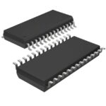 PI6C20400BLEX
The activity of extra discounts on wholesale prices is in full swing…
Please fill in your contact information and we will send you the latest wholesale price list.







