 ChipApex | Global Electronic Components Supplier
SEARCH
Search Product
Search Post
— IC芯片 | 连接器 | 传感器 | 被动器件 —
Search productSearch post
— IC芯片 | 连接器 | 传感器 | 被动器件 —
Consult the customer manager about the wholesale price.
consultation hotline:86-132-6715-2157
email:[email protected]
Contact the product manager for consultation. One-stop consultation is available.
Do you want a lower wholesale price? Please send us your inquiry and we will reply immediately.
The PI6C20400SLE is a PCIe-compatible high-speed, low-noise differential clock buffer manufactured by Diodes Incorporated. Designed as a companion to PCIe 3.0 clock generators, it distributes a single differential source clock into four pairs of differential outputs. The device supports LVTTL input and operates within a supply voltage range of 3.135V to 3.465V. It features an internal PLL for jitter reduction and provides flexible control via SRC_STOP#, PWRDWN#, and SMBus interfaces. Packaged in a 28-TSSOP case, it functions at frequencies up to 100MHz across a commercial temperature range of 0°C to 70°C.
Verify the package type matches the required 28-TSSOP footprint during integration. Confirm that the operating environment remains within the specified 0°C to 70°C range. Ensure power supply stability between 3.135V and 3.465V to maintain signal integrity. Check for RoHS compliance status if environmental regulations apply to the final assembly.
Select this component when a PCIe 3.0 compliant clock buffer with four differential outputs is required. It is suitable for designs needing low-noise clock distribution from a single source. Consider the LVTTL input requirement and the availability of SMBus control lines for dynamic configuration. Verify that the 100MHz maximum frequency meets the system timing requirements.
This part belongs to the Diodes Incorporated clock buffer family, specifically optimized for PCI Express applications. It serves as a critical timing element in systems requiring precise clock distribution to multiple endpoints. The device complements PCIe clock generators by providing fan-out and jitter cleaning capabilities essential for high-speed serial links.
Direct substitutes must support 1:4 differential output ratios and PCIe 3.0 compatibility. Verify pinout compatibility with the 28-TSSOP package. Ensure equivalent electrical characteristics, including supply voltage ranges and operating temperatures, are maintained for seamless integration.
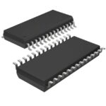 PI6C20400SLE
The activity of extra discounts on wholesale prices is in full swing…
Please fill in your contact information and we will send you the latest wholesale price list.






