 ChipApex | Global Electronic Components Supplier
SEARCH
Search Product
Search Post
— IC芯片 | 连接器 | 传感器 | 被动器件 —
Search productSearch post
— IC芯片 | 连接器 | 传感器 | 被动器件 —
Consult the customer manager about the wholesale price.
consultation hotline:86-132-6715-2157
email:[email protected]
Contact the product manager for consultation. One-stop consultation is available.
Do you want a lower wholesale price? Please send us your inquiry and we will reply immediately.
The PI6C20800SAEX is a PCI Express high-speed, low-noise differential clock buffer manufactured by Diodes Incorporated. It distributes the differential SRC clock from the PI6C410BS generator to eight differential pairs of HCSL outputs in a 48-TSSOP package. The device supports both PLL and fanout modes with an input frequency range up to 400 MHz in bypass mode. It operates on a single 3.3V supply (3.135V to 3.465V) within the commercial temperature range of 0°C to 70°C. Key electrical characteristics include output-to-output skew less than 50ps and cycle-to-cycle jitter under 70ps.
Verify the specific ordering suffix 'A' corresponds to the 48-pin TSSOP package and 'E' indicates lead-free/green compliance. Confirm that the base model PI6C20800S denotes the commercial temperature grade (0°C to 70°C), distinct from the industrial variant PI6C20800SI (-40°C to 85°C). Ensure the datasheet revision matches current manufacturing specifications.
Select this component when designing for Intel server chipsets requiring a companion to the PI6C410BS clock generator. Choose the PI6C20800SAEX over the SI variant if the application environment remains within the 0°C to 70°C commercial range. Verify that the required output skew specification is met by the <50ps characteristic of the standard S version rather than the <60ps of the SI version.
This part belongs to the PI6C20800S series of PCIe clock buffers. It is functionally similar to the PI6C20800VE but utilizes HCSL outputs instead of LVDS/LVPECL variants found in other family members. The 'A' suffix specifically identifies the TSSOP-48 package form factor used in this ordering code.
The PI6C20800SIAEX serves as the industrial temperature qualified replacement for this component. Direct substitution requires verifying that the -40°C to 85°C operating range is acceptable and that the package pinout remains identical.
The input frequency can be divided by 2 by pulling the SRC_DIV# pin LOW. When HIGH, the input passes through normally.
In bypass mode, the maximum input frequency is 400 MHz. In PLL mode, it is restricted to the 95 MHz to 105 MHz range.
Outputs can be enabled/disabled individually via SMBus Data Byte 1. They can also be globally tristated by asserting SRC_STOP# or PWRDWN# inputs LOW.
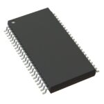 PI6C20800SAEX
The activity of extra discounts on wholesale prices is in full swing…
Please fill in your contact information and we will send you the latest wholesale price list.






