 ChipApex | Global Electronic Components Supplier

SEARCH
Search Product
Search Post
— IC芯片 | 连接器 | 传感器 | 被动器件 —
Search productSearch post
— IC芯片 | 连接器 | 传感器 | 被动器件 —
Consult the customer manager about the wholesale price.
consultation hotline:86-132-6715-2157
email:[email protected]
Contact the product manager for consultation. One-stop consultation is available.
Do you want a lower wholesale price? Please send us your inquiry and we will reply immediately.
PI6CB33402ZHIEX is listed in the Clock Buffers, Drivers range at ChipApex. The manufacturer field lists Diodes Incorporated. Its product description is IC CLK BUF 1:4 133.33MHZ 32TQFN. Review the specifications below when checking this part for your BOM.
The PI6CB33402 is a very low power 4-output PCIe clock buffer manufactured by Diodes Incorporated. It accepts a differential HCSL input and provides four low-power differential HCSL outputs with integrated on-chip termination, eliminating the need for external resistors. The device operates at a nominal 3.3V supply voltage and supports frequencies of 100MHz, 50MHz, 125MHz, and 133.33MHz via SMBus configuration. It features a proprietary PLL design to achieve very low jitter compliant with PCIe Gen 1 through Gen 5 standards. Key specifications include a maximum output frequency of 133.33MHz, an operating temperature range of -40°C to +85°C, and a 32-contact TQFN package.
Verify the specific ordering suffix against the datasheet to confirm tape orientation. The part number PI6CB33402ZHIEX corresponds to the 32-contact TQFN package with Pin 1 located at the top right corner. Ensure that the procurement documentation matches the required package code ZH and confirms RoHS compliance and lead-free status as specified by the manufacturer.
Select this component when a 1:4 fanout buffer with integrated termination is required to simplify PCB layout. It is suitable for designs needing support for multiple standard frequencies (50MHz, 100MHz, 125MHz, 133.33MHz) without external crystal changes. Consider the SMBus interface requirements for dynamic configuration of slew rate, amplitude, and PLL bandwidth if adaptive performance tuning is necessary for the target application.
This device belongs to the PI6CB33 series of clock buffers from Diodes Incorporated. It is designed to replace discrete resistor networks for HCSL termination, reducing component count and board space. The integration of the PLL allows for jitter cleaning and frequency multiplication/division capabilities within a single small footprint package.
Public confirmed substitute part numbers are not available in the provided source material.
The default on-chip termination impedance (ZOUT) is 85Ω.
The SMBus address is latched on the SADR_TRI pin upon the first high assertion of the PD# pin. The address can be selected using tri-level latching states.
Yes, the PLL operating mode can be set to bypass via the BW_SEL_TRI pin or SMBus. In bypass mode, the PLL is off, and inputs pass directly to the outputs.
Explore related parts through Clock/Timing, Integrated Circuits (ICs), all product categories, ChipApex homepage.
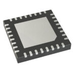 PI6CB33402ZHIEX

The activity of extra discounts on wholesale prices is in full swing…
Please fill in your contact information and we will send you the latest wholesale price list.







