 ChipApex | Global Electronic Components Supplier
SEARCH
Search Product
Search Post
— IC芯片 | 连接器 | 传感器 | 被动器件 —
Search productSearch post
— IC芯片 | 连接器 | 传感器 | 被动器件 —
Consult the customer manager about the wholesale price.
consultation hotline:86-132-6715-2157
email:[email protected]
Contact the product manager for consultation. One-stop consultation is available.
Do you want a lower wholesale price? Please send us your inquiry and we will reply immediately.
The PI6CV857LAE is a PLL-based clock buffer designed for registered DDR DIMM applications. It distributes one differential clock input pair to ten differential output pairs and one feedback pair. The device operates with AVDD and VDDQ supplies ranging from 2.3V to 2.7V, supporting SSTL-2 input and output levels. It features a maximum operating frequency of 170MHz and includes a PWRDWN control pin for power management. The component is housed in a 48-TSSOP package and functions within an operating temperature range of 0°C to 70°C.
Verify the specific ordering suffix 'E' confirms Pb-free and Green material compliance as defined in the manufacturer's documentation. Confirm that the 48-TSSOP package dimensions align with the target PCB footprint requirements. Ensure the design accommodates the 2.3V to 2.7V supply voltage range for both AVDD and VDDQ pins to maintain proper operation.
Select this component when a single differential clock source must drive multiple DDR memory devices with minimal skew. The internal PLL allows synchronization via external FBIN/FBIN pins. Consider the 0°C to 70°C commercial temperature grade against system thermal constraints. Verify compatibility with SSTL-2 signaling levels required by the target memory interface.
This part belongs to the PI6CV857 series of PLL clock drivers developed for high-performance memory applications. It serves as a zero-delay buffer to synchronize output clocks directly to the input reference. The device integrates power-down logic and supports spread spectrum clocking inputs to manage EMI in dense memory subsystems.
Public confirmed substitute part numbers are not available in the provided documentation.
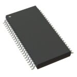 PI6CV857LAE
The activity of extra discounts on wholesale prices is in full swing…
Please fill in your contact information and we will send you the latest wholesale price list.






