 ChipApex | Global Electronic Components Supplier
SEARCH
Search Product
Search Post
— IC芯片 | 连接器 | 传感器 | 被动器件 —
Search productSearch post
— IC芯片 | 连接器 | 传感器 | 被动器件 —
Consult the customer manager about the wholesale price.
consultation hotline:86-132-6715-2157
email:[email protected]
Contact the product manager for consultation. One-stop consultation is available.
Do you want a lower wholesale price? Please send us your inquiry and we will reply immediately.
The PI6PCIEB24ZDE is a 1:4 PCI Express® 2.0 compliant differential clock driver manufactured by Diodes Incorporated (formerly Pericom). It distributes a single differential input clock to four differential output pairs using a zero-delay PLL. The device operates at 100 MHz with a 3.3V supply, delivering low skew (<50ps) and cycle-to-cycle jitter (<50ps). Additive RMS phase jitter is less than 1 ps. It features programmable output current via an external resistor, power-down control, and individual output enable pins for each bank.
Verify the package code ZD corresponds to the 20-pin TQFN (4.0mm x 4.0mm). Confirm RoHS compliance through the 'E' suffix in the ordering code. Ensure the specific revision matches the datasheet PS9070A dated 09/01/10 for accurate electrical characteristics.
Select this component when a 1:4 differential clock buffer with strict PCIe 2.0 jitter requirements is needed. It requires a 3.3V supply and an external resistor for IREF setting. Consider bypass mode if PLL functionality is not required for system testing.
This part belongs to the PI6PCIE series of high-speed clock drivers designed specifically for PCI Express standards. It serves as a buffer between a clock synthesizer (like the PI6C410) and multiple PCIe endpoints or switches.
Publicly confirmed substitute part numbers are not available in the provided documentation. Verify pinout compatibility and electrical specifications before considering alternative vendors.
The differential output current is determined by an external resistor connected to the IREF pin. For example, a 475Ω resistor sets the nominal current.
When HIGH, the internal PLL is enabled for normal operation. When LOW, the PLL is bypassed, allowing the input clock to pass directly to the outputs with a propagation delay of 2.5ns to 6.5ns.
Asserting PWRDWN# Low puts the device in power down mode, where 2xIREF current flows through the OUT pins, resulting in a low state.
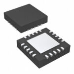 PI6PCIEB24ZDE
The activity of extra discounts on wholesale prices is in full swing…
Please fill in your contact information and we will send you the latest wholesale price list.





