 ChipApex | Global Electronic Components Supplier

SEARCH
Search Product
Search Post
— IC芯片 | 连接器 | 传感器 | 被动器件 —
Search productSearch post
— IC芯片 | 连接器 | 传感器 | 被动器件 —
Consult the customer manager about the wholesale price.
consultation hotline:86-132-6715-2157
email:[email protected]
Contact the product manager for consultation. One-stop consultation is available.
Do you want a lower wholesale price? Please send us your inquiry and we will reply immediately.
The PJS6601-AU is a complementary enhancement mode MOSFET pair manufactured by Panjit International Inc. The N-channel device provides a drain-source voltage of 20V and continuous current up to 4.1A, while the P-channel counterpart supports -20V and -3.1A. Both transistors utilize advanced trench process technology within an SOT-23 6L package. Key electrical parameters include a maximum on-resistance of 56mΩ for the N-channel at VGS=4.5V and 115mΩ for the P-channel at VGS=-4.5V. The components are qualified under AEC-Q101 standards and support operating junction temperatures from -55°C to +150°C.
Verify the specific ordering suffix against official Panjit documentation to confirm exact packing configurations. Confirm that the required lot number tracking aligns with manufacturer policies for warranty claims. Ensure component authenticity through authorized distribution channels to maintain AEC-Q101 compliance integrity.
Select this complementary pair when space-constrained designs require matched N-channel and P-channel switching capabilities. Evaluate the thermal resistance of 100°C/W against system dissipation requirements. Verify gate threshold voltages match the logic levels of the driving circuitry for reliable turn-on performance.
This component belongs to Panjit's automotive-grade MOSFET portfolio, specifically engineered for high-reliability environments. It integrates both transistor types into one footprint to simplify PCB layout and reduce assembly complexity compared to discrete solutions.
No public substitute part numbers are documented in the provided datasheet. Cross-reference pinouts and electrical limits carefully if considering alternative manufacturers.
The maximum continuous drain current for the N-channel device is 4.1A.
Yes, the component is AEC-Q101 qualified, indicating suitability for automotive electronic systems.
The typical total gate charge (Qg) for the N-channel device is 4.6nC under standard test conditions.
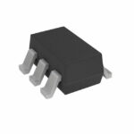 PJS6601-AU_S1_000A1

The activity of extra discounts on wholesale prices is in full swing…
Please fill in your contact information and we will send you the latest wholesale price list.





