 ChipApex | Global Electronic Components Supplier
SEARCH
Search Product
Search Post
— IC芯片 | 连接器 | 传感器 | 被动器件 —
Search productSearch post
— IC芯片 | 连接器 | 传感器 | 被动器件 —
Consult the customer manager about the wholesale price.
consultation hotline:86-132-6715-2157
email:[email protected]
Contact the product manager for consultation. One-stop consultation is available.
Do you want a lower wholesale price? Please send us your inquiry and we will reply immediately.
The PN4391 TRE is an N-channel silicon JFET from Central Semiconductor, packaged in TO-92 with a reel format. It features a maximum gate-drain voltage of 40 V and gate-source voltage of 40 V. The device supports a power dissipation of 625 mW and operates within a junction temperature range of -65 to +150 °C. Electrical characteristics include an IDSS range of 50 to 150 mA at VDS=20V, a VGS(OFF) range of 4.0 to 10 V, and an on-resistance (rDS(ON)) of up to 30 Ω at ID=1.0mA.
Verify the specific ordering suffix required for plating configuration when placing orders. The manufacturer specifies that adding the suffix TIN/LEAD requests tin/lead plated devices, while PBFREE indicates lead-free plating. Confirm the reel packaging quantity matches production requirements before finalizing procurement documentation.
Select this component based on its specified IDSS range of 50 to 150 mA and VGS(OFF) limits between 4.0 and 10 V. Ensure the circuit design accommodates the 625 mW power dissipation limit and the operating temperature range extending to +150 °C. Verify compatibility with the TO-92 through-hole mounting style.
This part belongs to the PN4391 series of N-channel silicon JFETs manufactured by Central Semiconductor Corp. The series includes variants such as PN4392 and PN4393, which share similar structural characteristics but differ in specific electrical thresholds like pinch-off voltage and drain current ranges.
Cross-reference with PN4392 or PN4393 if different VGS(OFF) or IDSS parameters are required. Verify pinout compatibility, as all series members utilize the same TO-92 lead configuration with Drain, Source, and Gate assignments.
The maximum power dissipation (PD) is rated at 625 mW at an ambient temperature of 25°C.
Lead 1 is the Drain, Lead 2 is the Source, and Lead 3 is the Gate.
The turn-on time (ton) is typically 15 ns when tested with an ID(ON) of 12 mA.
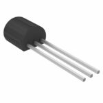 PN4391 TRE
The activity of extra discounts on wholesale prices is in full swing…
Please fill in your contact information and we will send you the latest wholesale price list.





