ChipApex | Global Electronic Components Supplier
SEARCH
Search Product
Search Post
— IC芯片 | 连接器 | 传感器 | 被动器件 —
Search productSearch post
— IC芯片 | 连接器 | 传感器 | 被动器件 —
Consult the customer manager about the wholesale price.
consultation hotline:86-132-6715-2157
email:[email protected]
Contact the product manager for consultation. One-stop consultation is available.
Do you want a lower wholesale price? Please send us your inquiry and we will reply immediately.
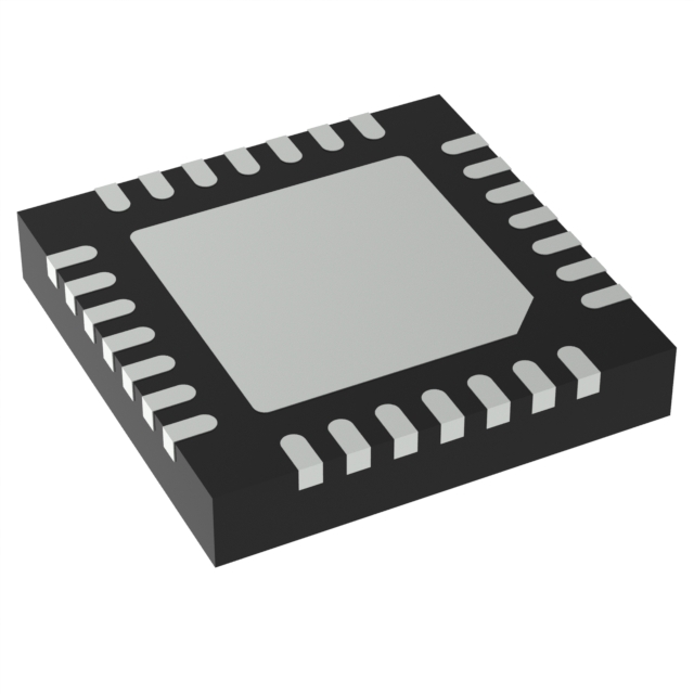
The RC19104AGNL#BB0 is a Renesas Electronics PCIe Gen7 compliant clock buffer operating at 1.8V with four differential outputs. It features ultra-low additive phase jitter, specified at 2.6fs RMS for PCIe Gen7 and 33fs RMS at 156.25MHz (12kHz to 20MHz). The device accepts HCSL or LVDS input signals and provides LP-HCSL outputs with selectable differential impedances of 33Ω, 85Ω, or 100Ω via pins or SMBus. Packaged in a 28-lead VFQFPN (4x4mm) case, it supports an operating temperature range of -40°C to +105°C.
Verify the specific suffix #BB0 against official documentation to confirm packaging details such as tray quantity or reel specifications. Ensure the 28-VFQFPN exposed pad package matches the target PCB footprint requirements. Confirm RoHS compliance status through the manufacturer's latest datasheet before finalizing procurement orders.
Select this component when designing for PCIe Gen7 signaling standards requiring minimal added jitter. The 1.8V supply voltage and LP-HCSL output type are critical for compatibility with modern server and accelerator architectures. Verify that the required output impedance configuration can be set via available control pins or SMBus interface.
This part belongs to the RC191xx family of 1.8V PCIe Gen7 buffers. It serves as a direct upgrade path for legacy designs using lower-generation PCIe clocks, offering improved jitter performance and flexible output drive capabilities while maintaining backward compatibility with earlier PCIe standards.
The RC19108A series offers eight outputs instead of four. For three-output configurations, consider the RC19103A variant. Ensure any replacement maintains the 1.8V supply requirement and compatible package dimensions.
 RC19104AGNL#BB0
The activity of extra discounts on wholesale prices is in full swing…
Please fill in your contact information and we will send you the latest wholesale price list.