 ChipApex | Global Electronic Components Supplier
SEARCH
Search Product
Search Post
— IC芯片 | 连接器 | 传感器 | 被动器件 —
Search productSearch post
— IC芯片 | 连接器 | 传感器 | 被动器件 —
Consult the customer manager about the wholesale price.
consultation hotline:86-132-6715-2157
email:[email protected]
Contact the product manager for consultation. One-stop consultation is available.
Do you want a lower wholesale price? Please send us your inquiry and we will reply immediately.
The Vishay Siliconix SI3590DV-T1-GE3 is a dual N- and P-channel MOSFET in a TSOP-6 package. It features TrenchFET technology for ultra-low on-resistance, optimized for high-side and low-side switching applications to minimize conduction losses. The N-channel device supports a drain-source voltage of 30 V with a typical RDS(on) of 0.077 Ω at VGS = 4.5 V and a continuous drain current of 3 A. The P-channel counterpart offers -30 V breakdown with a typical RDS(on) of 0.170 Ω at VGS = -4.5 V and a continuous drain current of -2 A. Both channels share a maximum junction temperature range of -55 °C to +150 °C.
Verify the ordering suffix 'GE3' confirms lead-free and halogen-free compliance status as specified in the manufacturer's documentation. Ensure the component matches the TSOP-6 package dimensions and pinout configuration required by the target PCB layout. Cross-reference the specific document revision number against the latest official datasheet to confirm no parameter updates have occurred since publication.
Select this dual MOSFET when space-constrained designs require complementary N- and P-channel switching in a single footprint. Evaluate thermal resistance ratings against the expected ambient temperature and duty cycle to ensure junction temperatures remain within the -55 °C to +150 °C operating range. Confirm that the gate drive voltage levels are sufficient to achieve the specified low on-resistance values for efficient power management.
This component belongs to the Vishay Siliconix Si3590 series of dual MOSFETs. It utilizes the TSOP-6 surface-mount package, which is standardized under JEDEC MO-193C. The device integrates separate N-channel and P-channel structures on a single substrate, designed specifically for portable electronics where board area and switching efficiency are critical constraints.
Consult official Vishay documentation for confirmed substitute part numbers. Verify pin compatibility and electrical specifications before substituting any alternative components.
The maximum pulsed drain current (IDM) is 8 A for the N-channel and 8 A for the P-channel.
The gate threshold voltage (VGS(th)) ranges from 0.6 V to 1.5 V for the N-channel and -0.6 V to -1.5 V for the P-channel, tested at ID = ±250 μA.
The on-resistance increases with junction temperature. Typical characteristics show normalized RDS(on) rising significantly as temperature increases from -55 °C to +150 °C.
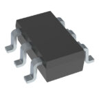 SI3590DV-T1-GE3
The activity of extra discounts on wholesale prices is in full swing…
Please fill in your contact information and we will send you the latest wholesale price list.





