 ChipApex | Global Electronic Components Supplier
SEARCH
Search Product
Search Post
— IC芯片 | 连接器 | 传感器 | 被动器件 —
Search productSearch post
— IC芯片 | 连接器 | 传感器 | 被动器件 —
Consult the customer manager about the wholesale price.
consultation hotline:86-132-6715-2157
email:[email protected]
Contact the product manager for consultation. One-stop consultation is available.
Do you want a lower wholesale price? Please send us your inquiry and we will reply immediately.
The SI52143-A01AGMR is a PCIe clock generator providing four differential outputs and one single-ended reference clock. It supports PCI-Express Gen 1, 2, 3, and 4 common clock standards, as well as Gen 3 SRNS compliance. The device accepts a 25 MHz crystal or clock input and generates 100 MHz differential clocks with a 0.7 V crossing point voltage. Operating on a 3.3 V supply (3.135 V to 3.465 V), it features I2C programmability for dynamic control of skew, edge rate, and amplitude. The component is housed in a 24-pin QFN package and operates within an industrial temperature range of -40 °C to +85 °C.
Verify the 'R' suffix indicates tape and reel packaging rather than tray packaging. Confirm the specific revision code matches system requirements via I2C readback. Ensure ESD handling protocols are followed due to the sensitivity of the CMOS inputs and high-frequency outputs.
Select this model when Gen 4 compliance or SRNS support is required. Use the A01A variant for standard 100 MHz differential outputs. Verify that the application can accommodate the 24-pin QFN land pattern dimensions. Ensure the design includes appropriate termination for HCSL signaling levels if LVDS or CML compatibility is needed.
This part belongs to the Si52143 family of PCIe clock generators. The -A01AGM designation represents the tray-packaged version, while the -R suffix specifically denotes the tape and reel packaging format intended for automated surface-mount assembly processes.
The SI52143-A01AGM is functionally identical but utilizes tray packaging instead of tape and reel.
Spread spectrum is enabled by driving the SSON pin logic high. This activates a -0.5% down-spread profile on all differential outputs.
For PCIe Gen 3 phase jitter with a common clock, the maximum RMS value is 0.9 ps when measured with a PLL bandwidth of 2–4 or 2–5 MHz and a CDR of 10 MHz.
Yes, individual outputs can be enabled or disabled using dedicated hardware OE pins or through I2C register programming.
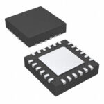 SI52143-A01AGMR
The activity of extra discounts on wholesale prices is in full swing…
Please fill in your contact information and we will send you the latest wholesale price list.






