 ChipApex | Global Electronic Components Supplier
SEARCH
Search Product
Search Post
— IC芯片 | 连接器 | 传感器 | 被动器件 —
Search productSearch post
— IC芯片 | 连接器 | 传感器 | 被动器件 —
Consult the customer manager about the wholesale price.
consultation hotline:86-132-6715-2157
email:[email protected]
Contact the product manager for consultation. One-stop consultation is available.
Do you want a lower wholesale price? Please send us your inquiry and we will reply immediately.
The Si52202-A01AGM is a two-output PCI Express clock generator supporting Gen 1 through Gen 7 and SRIS architectures. It provides two 100 MHz differential LP-HCSL outputs compliant with PCIe common clock and separate reference specifications. The device operates on a 1.5 V to 1.8 V supply with separate VDD and VDD_IO rails. Key electrical parameters include a maximum RMS jitter of 0.085 ps, an operating temperature range of –40 °C to +85 °C, and a 20-pin QFN (3 x 3 mm) package. It accepts a 25 MHz crystal or clock input.
Verify the specific ordering suffix against the manufacturer's current documentation to confirm package type and termination resistance values. Confirm RoHS compliance status via the official Certificate of Conformance. Ensure the selected variant matches the required internal impedance termination for the target PCB trace design.
Select this component for designs requiring only two differential PCIe clock outputs in a minimal footprint. The Si52202 utilizes a 20-pin QFN package, which is the smallest in its family. Verify that the application does not require the Wake-on LAN power-down feature, as this function is explicitly excluded for the Si52202 model compared to higher-output variants.
The Si52202 belongs to the Si522xx family, which also includes the Si52212 (12 outputs), Si52208 (8 outputs), and Si52204 (4 outputs). While sharing similar core PLL and control features, the Si52202 is distinct in offering only two differential outputs and lacking the LVCMOS reference clock output found in other family members.
Direct functional replacements within the same package are limited due to the unique pinout of the 20-pin QFN. Higher-output variants like the Si52204 or Si52208 require significant schematic and layout modifications. Consult Skyworks Solutions for specific cross-reference recommendations.
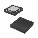 SI52202-A01AGM
The activity of extra discounts on wholesale prices is in full swing…
Please fill in your contact information and we will send you the latest wholesale price list.






