 ChipApex | Global Electronic Components Supplier
SEARCH
Search Product
Search Post
— IC芯片 | 连接器 | 传感器 | 被动器件 —
Search productSearch post
— IC芯片 | 连接器 | 传感器 | 被动器件 —
Consult the customer manager about the wholesale price.
consultation hotline:86-132-6715-2157
email:[email protected]
Contact the product manager for consultation. One-stop consultation is available.
Do you want a lower wholesale price? Please send us your inquiry and we will reply immediately.
The Si5324D-C-GM is a low-bandwidth, jitter-attenuating precision clock multiplier utilizing Skyworks' 3rd-generation DSPLL technology. It accepts two input clocks from 2 kHz to 710 MHz and generates two independent output clocks ranging from 2 kHz to 945 MHz, with select frequencies reaching 1.4 GHz. The device features digitally programmable loop bandwidths between 4 Hz and 525 Hz and supports LVPECL, LVDS, CML, and CMOS output formats. It operates on a single supply of 1.8 V ±5%, 2.5 V ±10%, or 3.3 V ±10% within an ambient temperature range of -40 °C to +85 °C.
Verify the specific speed grade suffix (e.g., D) against the datasheet ordering guide to ensure compliance with required frequency limits and timing specifications. Confirm that the QFN-36 package land pattern matches the PCB design requirements. Ensure power supply decoupling capacitors are placed close to the VDD pins as shown in typical application circuits.
Select this component for applications requiring sub-1 ps jitter performance with narrow loop bandwidths. Verify that the input clock frequencies fall within the 2 kHz to 710 MHz range. Check if the required output format (LVPECL, LVDS, CML, or CMOS) aligns with the system interface. Note that LVPECL outputs require a nominal VDD of at least 2.5 V.
The Si5324 belongs to the Si53xx family of any-frequency jitter attenuating clock ICs. It is designed to eliminate the need for external VCXO and filter components by integrating the loop filter and PLL functions. The device provides flexible frequency translation capabilities suitable for high-performance timing applications across telecommunications and data converter domains.
Public confirmed substitute part numbers are not available in the provided documentation.
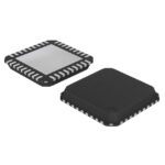 SI5324D-C-GM
The activity of extra discounts on wholesale prices is in full swing…
Please fill in your contact information and we will send you the latest wholesale price list.







