ChipApex | Global Electronic Components Supplier
SEARCH
Search Product
Search Post
— IC芯片 | 连接器 | 传感器 | 被动器件 —
Search productSearch post
— IC芯片 | 连接器 | 传感器 | 被动器件 —
Consult the customer manager about the wholesale price.
consultation hotline:86-132-6715-2157
email:[email protected]
Contact the product manager for consultation. One-stop consultation is available.
Do you want a lower wholesale price? Please send us your inquiry and we will reply immediately.
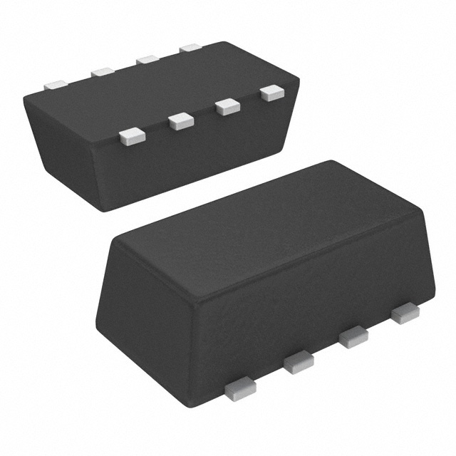
The SI5504BDC-T1-GE3 is a dual N- and P-channel MOSFET in a leadless 1206-8 ChipFET package. It features TrenchFET technology with a drain-source voltage of 30 V for the N-channel and -30 V for the P-channel. The N-channel has a maximum on-resistance of 0.065 Ω at VGS = 10 V and a continuous drain current of 4 A (TC = 25 °C). The P-channel exhibits a maximum on-resistance of 0.140 Ω at VGS = -10 V and a continuous drain current of -3.7 A (TC = 25 °C). The device operates within a junction temperature range of -55 °C to 150 °C.
Verify the specific ordering suffix GE3 to confirm the component is both lead-free and halogen-free, as distinct from the standard E3 variant which is only lead-free. Ensure the datasheet revision matches the required manufacturing date, as Vishay documents are subject to change without notice. Confirm that the leadless package singulation process requirements align with the assembly capabilities, particularly regarding exposed copper tips.
Select this component when space-constrained designs require dual-channel switching capabilities in a small surface-mount form factor. Evaluate the thermal resistance characteristics against the available PCB copper area, as the junction-to-ambient resistance is highly dependent on the pad pattern and board size. Verify that the gate threshold voltage and total gate charge parameters meet the drive requirements of the control circuitry.
This part belongs to the Vishay Siliconix Si5504 series of dual-channel MOSFETs. It is manufactured using silicon technology and utilizes the 1206-8 ChipFET package, which shares the same outline dimensions as common 1206 passive components but offers power semiconductor performance. The marking code for the device is EF.
The SI5504BDC-T1-E3 is a verified substitute that shares identical electrical specifications and package dimensions, differing only in the absence of the halogen-free compliance indicated by the GE3 suffix.
The typical junction-to-foot thermal resistance is 30 °C/W, with a maximum rating of 40 °C/W.
The 1206-8 ChipFET package achieves steady-state junction-to-ambient thermal resistance values identical to the SO-8 package on a 1-inch square FR4 board, despite having a significantly smaller body area.
Manual soldering with a soldering iron is not recommended for this leadless component due to the specific construction of the exposed copper terminals.
 SI5504BDC-T1-GE3
The activity of extra discounts on wholesale prices is in full swing…
Please fill in your contact information and we will send you the latest wholesale price list.