ChipApex | Global Electronic Components Supplier
SEARCH
Search Product
Search Post
— IC芯片 | 连接器 | 传感器 | 被动器件 —
Search productSearch post
— IC芯片 | 连接器 | 传感器 | 被动器件 —
Consult the customer manager about the wholesale price.
consultation hotline:86-132-6715-2157
email:[email protected]
Contact the product manager for consultation. One-stop consultation is available.
Do you want a lower wholesale price? Please send us your inquiry and we will reply immediately.
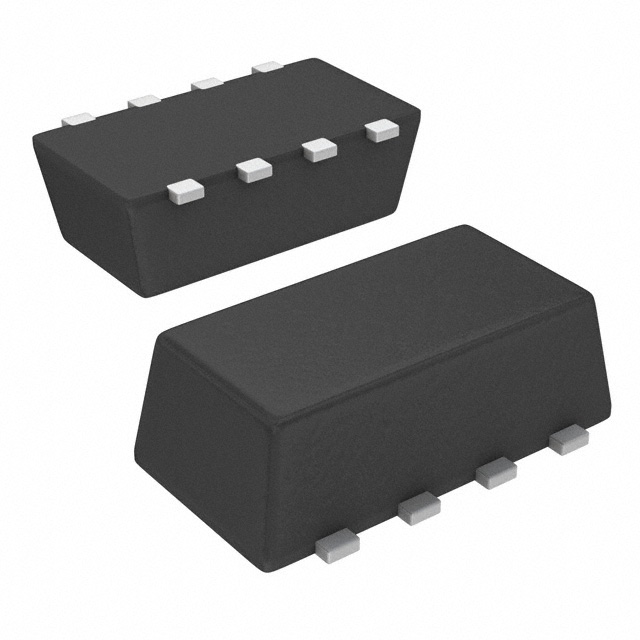
The Vishay Siliconix SI5915BDC-T1-GE3 is a dual P-channel MOSFET utilizing TrenchFET technology, housed in a leadless 1206-8 ChipFET package. It features an 8 V drain-source voltage rating and a continuous drain current of -4 A at 25 °C case temperature. The on-state resistance (RDS(on)) is specified as 0.070 Ω at VGS = -4.5 V and ID = -3.3 A, with a typical total gate charge (Qg) of 4 nC. Thermal performance includes a maximum junction-to-ambient thermal resistance of 74 °C/W and a steady-state junction-to-foot resistance of 40 °C/W. The device operates within a junction temperature range of -55 °C to +150 °C.
Verify the specific ordering suffix when sourcing components. The GE3 designation indicates lead-free and halogen-free compliance, whereas the E3 suffix denotes lead-free status only. Confirm that the required environmental specifications align with the exact suffix ordered to ensure material consistency during assembly.
Select this component for designs constrained by board space due to its 1206-8 footprint. Ensure the gate drive voltage meets the minimum threshold for the desired RDS(on), as resistance increases significantly below -4.5 V. Account for the package-limited current rating when designing high-current paths, as thermal dissipation may restrict continuous operation below the absolute maximum ratings.
This part belongs to the Vishay Siliconix Si5915BDC series of dual P-channel MOSFETs. It is manufactured using advanced silicon die technologies and utilizes the ChipFET leadless package format. The product line emphasizes miniaturization and thermal efficiency for mobile and battery-powered consumer electronics.
Direct functional replacements must match the dual P-channel topology, 8 V rating, and 1206-8 package dimensions. Verify pinout compatibility and thermal characteristics before substitution. Cross-referencing with other Vishay dual MOSFETs in the same package family is recommended for equivalent performance.
The E3 suffix indicates the component is lead-free. The GE3 suffix indicates the component is both lead-free and halogen-free, complying with IEC 61249-2-21 definitions.
RDS(on) increases as the gate-source voltage decreases. It is 0.070 Ω max at VGS = -4.5 V, 0.104 Ω max at VGS = -2.5 V, and 0.145 Ω max at VGS = -1.8 V.
No, manual soldering with a soldering iron is not recommended for this leadless component. Reflow soldering profiles should be followed to ensure adequate interconnection.
 SI5915BDC-T1-GE3
The activity of extra discounts on wholesale prices is in full swing…
Please fill in your contact information and we will send you the latest wholesale price list.