ChipApex | Global Electronic Components Supplier
SEARCH
Search Product
Search Post
— IC芯片 | 连接器 | 传感器 | 被动器件 —
Search productSearch post
— IC芯片 | 连接器 | 传感器 | 被动器件 —
Consult the customer manager about the wholesale price.
consultation hotline:86-132-6715-2157
email:[email protected]
Contact the product manager for consultation. One-stop consultation is available.
Do you want a lower wholesale price? Please send us your inquiry and we will reply immediately.
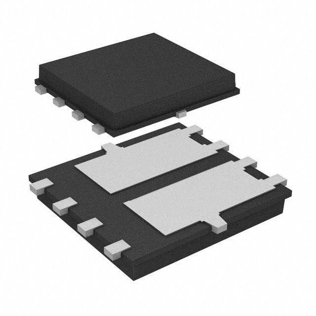
The Si7922DN-T1-E3 is a dual N-channel MOSFET from Vishay Siliconix, utilizing TrenchFET technology. It features a PowerPAK 1212-8 package with dimensions of 3.30 mm x 3.30 mm. The device has a drain-source voltage (VDS) rating of 100 V and a gate-source voltage (VGS) limit of ± 20 V. At VGS = 10 V, the maximum on-state resistance (RDS(on)) is 0.195 Ω at a continuous drain current (ID) of 2.5 A. At VGS = 6 V, RDS(on) is 0.230 Ω at an ID of 2.3 A. The maximum power dissipation is 2.6 W at TA = 25 °C. The operating junction temperature range spans from -55 °C to +150 °C.
Verify the specific ordering suffix when purchasing components. The E3 suffix indicates lead-free construction. The GE3 suffix denotes both lead-free and halogen-free compliance. Confirm that the required environmental specifications align with the selected variant before finalizing procurement orders.
Select this component for designs requiring high-voltage isolation in a minimal footprint. Evaluate the thermal requirements against the specified junction-to-ambient resistance values. Ensure the gate drive voltage supports the desired on-resistance characteristics, as performance varies between 6 V and 10 V gate biases.
This part belongs to the Vishay Siliconix Si79xx series of dual MOSFETs. It utilizes the PowerPAK 1212-8 package, which offers a significantly smaller footprint than standard SO-8 packages while maintaining similar thermal dissipation capabilities through direct die attachment to the substrate.
Check for availability of the halogen-free variant, Si7922DN-T1-GE3, if environmental regulations require it. Verify pinout compatibility if substituting with other dual MOSFETs in the same package family.
The Si7922DN-T1-E3 is lead-free, whereas the Si7922DN-T1-GE3 is both lead-free and halogen-free.
At VGS = 10 V, the maximum RDS(on) is 0.195 Ω. At VGS = 6 V, the maximum RDS(on) increases to 0.230 Ω.
 SI7922DN-T1-E3
The activity of extra discounts on wholesale prices is in full swing…
Please fill in your contact information and we will send you the latest wholesale price list.