 ChipApex | Global Electronic Components Supplier
SEARCH
Search Product
Search Post
— IC芯片 | 连接器 | 传感器 | 被动器件 —
Search productSearch post
— IC芯片 | 连接器 | 传感器 | 被动器件 —
Consult the customer manager about the wholesale price.
consultation hotline:86-132-6715-2157
email:[email protected]
Contact the product manager for consultation. One-stop consultation is available.
Do you want a lower wholesale price? Please send us your inquiry and we will reply immediately.
The ALD110800APCL is a monolithic quad N-Channel Zero Threshold MOSFET array manufactured by Advanced Linear Devices Inc. utilizing EPAD CMOS technology. It features four matched pairs in a 16-pin Plastic DIP package with an operating temperature range of 0°C to +70°C. Key electrical parameters include a Drain-Source Breakdown Voltage (BVDSX) of 10V, Gate-Source voltage limits of ±10.6V, and maximum power dissipation of 500mW. The threshold voltage (VGS(th)) is precisely set at 0.00V with a maximum offset of 10mV. On-resistance is specified as 500Ω at VGS=4.0V and approximately 104kΩ at VGS=0.0V.
Verify the specific suffix 'PCL' corresponds to the 16-pin Plastic DIP package configuration when sourcing components. Confirm that the RoHS compliance status aligns with project requirements, as indicated by the 'L' suffix designation in the manufacturer's ordering information. Ensure the operating temperature range meets the environmental constraints of the intended deployment scenario.
Select this component for designs requiring precise matching between multiple N-channel devices on a single die. The zero threshold characteristic makes it suitable for sub-threshold operation and extremely low supply voltage environments. Consider the 16-pin PDIP package for through-hole assembly needs where space allows, noting the thermal dissipation limits inherent to this package type.
This device belongs to the EPAD® Matched Pair MOSFET Family from Advanced Linear Devices. It shares core technology with the ALD110900 series but differs in channel count and package options. The ALD110800 specifically denotes the quad configuration, while the APCL suffix identifies the plastic DIP variant within the broader product line designed for precision analog applications.
Direct replacements must maintain the zero threshold specification and quad N-channel configuration. Verify pinout compatibility for the 16-pin DIP package. Alternative parts from other manufacturers may require significant circuit redesign due to differences in threshold voltage programming and matching tolerances.
The typical offset voltage (VOS) is 1.8mV to 3.8mV, with a maximum specified value of 10mV.
At VGS = 0.0V, the device exhibits a nominal on-resistance of approximately 104kΩ, allowing it to function as a high-value resistor or switch with minimal leakage.
The Drain-Source Breakdown Voltage (BVDSX) is specified at 10V under conditions where V- = VGS = -1.0V and IDS = 1.0µA.
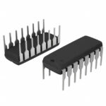 ALD110800APCL
The activity of extra discounts on wholesale prices is in full swing…
Please fill in your contact information and we will send you the latest wholesale price list.





