 ChipApex | Global Electronic Components Supplier
SEARCH
Search Product
Search Post
— IC芯片 | 连接器 | 传感器 | 被动器件 —
Search productSearch post
— IC芯片 | 连接器 | 传感器 | 被动器件 —
Consult the customer manager about the wholesale price.
consultation hotline:86-132-6715-2157
email:[email protected]
Contact the product manager for consultation. One-stop consultation is available.
Do you want a lower wholesale price? Please send us your inquiry and we will reply immediately.
The ALD1101ASAL is a monolithic dual N-channel matched MOSFET pair manufactured using an enhanced ACMOS silicon gate process. It features a drain-source voltage of 10V, power dissipation of 500mW, and operates within a temperature range of 0°C to +70°C. The device offers low threshold voltages (0.4V to 1.0V depending on grade), high input impedance of 10^12Ω typical, and negative current temperature coefficient. Electrical characteristics include a maximum gate leakage current of 100pA at room temperature and input capacitance of 6-10pF.
Verify the specific offset voltage grade required for the application, as the ALD1101 series includes A, B, and standard grades with different Vos specifications. Confirm that the SOIC-8 package aligns with the PCB footprint requirements. Ensure static control procedures are followed during handling due to ESD sensitivity. Check RoHS compliance status if manufacturing in restricted regions.
Select the appropriate grade based on offset voltage requirements: ALD1101A for 2mV, ALD1101B for 5mV, or standard ALD1101 for 10mV. Consider the trade-off between threshold voltage and mismatch when choosing between grades. Verify that the 10V breakdown voltage meets the system supply constraints. Evaluate input capacitance requirements for high-frequency switching applications.
The ALD1101 is part of Advanced Linear Devices' dual matched MOSFET family, designed specifically for precision analog signal processing. It complements the P-channel ALD1102 to form complete CMOS analog switches. The device utilizes ACMOS technology to achieve extremely high DC current gain and low leakage currents suitable for sensitive measurement systems.
No direct public substitute part numbers are documented in the provided datasheet. Designers should evaluate other dual N-channel MOSFET pairs with similar 10V ratings and low Vos specifications if replacement is necessary.
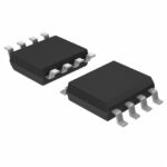 ALD1101ASAL
The activity of extra discounts on wholesale prices is in full swing…
Please fill in your contact information and we will send you the latest wholesale price list.





