ChipApex | Global Electronic Components Supplier
SEARCH
Search Product
Search Post
— IC芯片 | 连接器 | 传感器 | 被动器件 —
Search productSearch post
— IC芯片 | 连接器 | 传感器 | 被动器件 —
Consult the customer manager about the wholesale price.
consultation hotline:86-132-6715-2157
email:[email protected]
Contact the product manager for consultation. One-stop consultation is available.
Do you want a lower wholesale price? Please send us your inquiry and we will reply immediately.
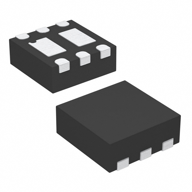
The SiA950DJ-T1-GE3 is a dual N-channel enhancement mode MOSFET from Vishay Siliconix, utilizing TrenchFET technology. It features a maximum drain-source voltage (VDS) of 190 V and a continuous drain current (ID) of 0.95 A at TC = 25 °C. The device is housed in a thermally enhanced PowerPAK SC-70-6 package with a thin 0.75 mm profile. Key electrical parameters include a typical total gate charge (Qg) of 1.4 nC at VGS = 10 V, and a maximum on-state resistance (RDS(on)) of 3.8 Ω at VGS = 4.5 V. Operating junction temperature ranges from -55 °C to +150 °C.
Verify the component authenticity by checking the manufacturer's datasheet document number 64712 and revision history. Confirm that the ordering suffix matches the specified lead-free and halogen-free requirements. Ensure compatibility with standard surface mount assembly processes and verify thermal pad soldering recommendations for the specific PCB layout.
Select this component when designing circuits requiring dual isolated channels with high voltage tolerance in a minimal footprint. Evaluate the RDS(on) limits against expected load currents to ensure acceptable power dissipation. Consider the low gate charge for driving efficiency in battery-operated systems where minimizing control power is critical.
This part belongs to the SiA series of dual MOSFETs designed for space-constrained portable electronics. It represents an evolution in TrenchFET technology aimed at reducing on-resistance while maintaining high voltage ratings. The PowerPAK SC-70 package provides a balance between thermal performance and board area efficiency compared to traditional small outline packages.
No direct public substitute part numbers are documented in the provided source material. Designers should consult official replacement guides or contact authorized distributors for cross-reference information if obsolescence occurs.
 SIA950DJ-T1-GE3
The activity of extra discounts on wholesale prices is in full swing…
Please fill in your contact information and we will send you the latest wholesale price list.