ChipApex | Global Electronic Components Supplier

SEARCH
Search Product
Search Post
— IC芯片 | 连接器 | 传感器 | 被动器件 —
Search productSearch post
— IC芯片 | 连接器 | 传感器 | 被动器件 —
Consult the customer manager about the wholesale price.
consultation hotline:86-132-6715-2157
email:[email protected]
Contact the product manager for consultation. One-stop consultation is available.
Do you want a lower wholesale price? Please send us your inquiry and we will reply immediately.
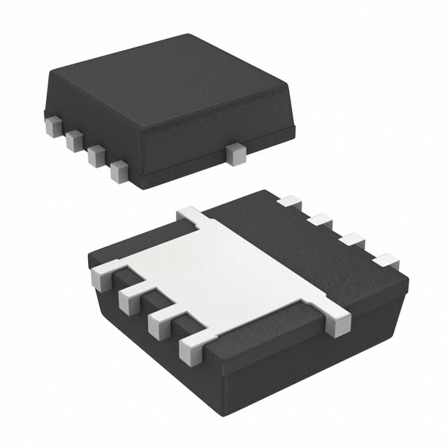
SIS606BDN-T1-GE3 is listed in the Single FETs, MOSFETs range at ChipApex. The manufacturer field lists Vishay Siliconix. Its product description is MOSFET N-CH 100V 9.4A/35.3A PPAK. Review the specifications below when checking this part for your BOM.
The SIS606BDN-T1-GE3 is a Vishay Siliconix N-channel MOSFET featuring TrenchFET Gen IV technology. It operates with a drain-source voltage of 100 V and a continuous drain current of 35.3 A at TC = 25 °C. The device offers a maximum on-resistance of 0.0174 Ω at VGS = 10 V and 0.0205 Ω at VGS = 7.5 V. Typical gate charge is 15.1 nC at VGS = 7.5 V. It is housed in a leadless PowerPAK 1212-8 package, rated for junction temperatures from -55 °C to +150 °C.
Verify component authenticity by cross-referencing the manufacturer part number SIS606BDN-T1-GE3 with official Vishay documentation. Confirm compliance with RoHS and REACH standards as specified in the datasheet. Ensure the ordering suffix matches the required lead-free and halogen-free configuration. Validate that the PowerPAK 1212-8 package dimensions align with your PCB footprint requirements before finalizing procurement.
Select this component for applications requiring high efficiency and low conduction losses within a compact surface-mount form factor. The optimized figure-of-merits make it suitable for high-frequency switching environments. Consider the thermal resistance ratings when designing heat dissipation strategies, particularly for synchronous rectification or motor drive scenarios where continuous current handling is critical.
This part belongs to the SiS series of N-channel MOSFETs manufactured by Vishay Siliconix. It utilizes advanced TrenchFET technology to achieve superior performance metrics compared to standard planar devices. The PowerPAK 1212-8 package provides a small footprint while maintaining robust electrical characteristics, positioning it as a solution for modern, space-constrained power management designs.
Consult official Vishay substitution guides for verified alternatives. Do not assume pin-compatible replacements without verifying absolute maximum ratings and thermal characteristics against the original specifications.
The absolute maximum gate-source voltage (VGS) is ±20 V.
Yes, the datasheet specifies that 100% of units are tested for Rg and Unclamped Inductive Switching (UIS).
The typical output capacitance (Coss) is 132 pF, measured at VDS = 50 V, VGS = 0 V, and f = 1 MHz.
Explore related parts through FETs, MOSFETs, Transistors, Discrete Semiconductor Products, all product categories.
 SIS606BDN-T1-GE3

The activity of extra discounts on wholesale prices is in full swing…
Please fill in your contact information and we will send you the latest wholesale price list.