 ChipApex | Global Electronic Components Supplier

SEARCH
Search Product
Search Post
— IC芯片 | 连接器 | 传感器 | 被动器件 —
Search productSearch post
— IC芯片 | 连接器 | 传感器 | 被动器件 —
Consult the customer manager about the wholesale price.
consultation hotline:86-132-6715-2157
email:[email protected]
Contact the product manager for consultation. One-stop consultation is available.
Do you want a lower wholesale price? Please send us your inquiry and we will reply immediately.
SMP1325-085LF is listed in the RF Diode range at ChipApex. The manufacturer field lists Skyworks Solutions Inc.. Its product description is RF DIODE PIN 200V 4.5W 3QFN. Review the specifications below when checking this part for your BOM.
The SMP1325-085LF is a surface-mount silicon PIN diode designed for high-power, high-volume switch and attenuator applications from 10 MHz to beyond 6 GHz. It features a maximum resistance of 0.5 Ω at 100 mA and a maximum capacitance of 0.65 pF at 20 V. The device has a 4.5 W dissipation power rating, capable of handling over 100 W continuous wave (CW) and 1000 W peak in a shunt-connected transmit/receive switch. It operates within an ambient temperature range of -40 °C to +150 °C.
Verify the specific ordering suffix against official Skyworks documentation before procurement. Confirm that the component meets RoHS3 compliance standards and check the latest Moisture Sensitivity Level (MSL) ratings. Ensure proper ESD precautions are implemented during handling and storage to prevent damage to the semiconductor die.
Select this component when low parasitic inductance and high power handling are required in RF circuits. The QFN package design reduces the effects of bond wire inductance compared to other surface-mount packages. Verify that the application frequency range falls between 10 MHz and beyond 6 GHz for optimal performance characteristics.
This part belongs to the Skyworks Solutions Inc. SMP1325 series of surface-mountable PIN diodes. It is specifically engineered as a shunt-connected device for high-power applications. The product utilizes a 3-pin, 2 x 2 mm QFN package to achieve low thermal resistance and minimal electrical parasitics.
No public confirmed substitute part numbers are available in the provided documentation.
The typical capacitance is 0.56 pF at 20 V reverse bias.
The QFN package produces lower thermal resistance and reduces the effects of parasitic inductance from anode bond wires compared to other surface-mount packages.
It is recommended to place several vias under the entire footprint of the exposed paddle (Pin 2) to minimize both electrical inductance to system ground and thermal resistance to the heat sink.
Explore related parts through Diodes, Discrete Semiconductor Products, all product categories, ChipApex homepage.
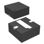 SMP1325-085LF

The activity of extra discounts on wholesale prices is in full swing…
Please fill in your contact information and we will send you the latest wholesale price list.




