 ChipApex | Global Electronic Components Supplier
SEARCH
Search Product
Search Post
— IC芯片 | 连接器 | 传感器 | 被动器件 —
Search productSearch post
— IC芯片 | 连接器 | 传感器 | 被动器件 —
Consult the customer manager about the wholesale price.
consultation hotline:86-132-6715-2157
email:[email protected]
Contact the product manager for consultation. One-stop consultation is available.
Do you want a lower wholesale price? Please send us your inquiry and we will reply immediately.
The SMP4393TR is an N-Channel JFET from the InterFET 2N4391-2-3 series, utilizing N0132S geometry for low noise and fast switching. It features a -40V gate-to-source breakdown voltage (BV_GSS) and a typical noise figure of 1.2 nV/√Hz. The device exhibits a drain-to-source saturation current (I_DSS) range of 5 to 30 mA and a gate-to-source cutoff voltage (V_GS(off)) between -0.5 V and -3.0 V. Static on-resistance (R_DS(on)) ranges from 30 to 100 Ω at 1 kHz. Dynamic characteristics include a turn-on delay of 15 ns and rise time of 5 ns. Input capacitance is 14 pF, while reverse transfer capacitance is 3.5 pF.
Verify the specific suffix TR indicates tape and reel packaging configuration as documented in the ordering information section. Confirm that the component meets RoHS compliance requirements before integration. Ensure design validation covers all field use cases and extreme conditions, as application responsibility rests with the buyer. Cross-reference the SOT23 package dimensions against JEDEC standards for proper PCB layout implementation.
Select this component when low noise and fast switching are critical for analog signal processing. The low cutoff voltage makes it suitable for low-level power supply applications compared to higher threshold variants. Consider the SOT23 surface mount package for space-constrained designs. Evaluate the specific I_DSS and V_GS(off) ranges required for the target circuit biasing conditions.
This part belongs to the InterFET 2N4391, 2N4392, and 2N4393 family of N-Channel JFETs. The SMP4393TR specifically denotes the surface mount version in SOT23 packaging supplied in tape and reel format. Other family members include through-hole TO-18 and TO-92 packages, as well as bare die options for specialized integration needs.
Direct substitutes within the same family include SMP4391TR and SMP4392TR, which share identical packaging but differ in electrical parameters such as I_DSS and V_GS(off). Through-hole equivalents are available as 2N4393 or PN4393. Verify pinout compatibility and electrical limits before substitution.
The typical noise figure is 1.2 nV/√Hz.
The maximum gate-to-source breakdown voltage (BV_GSS) is -40 V.
The input capacitance (C_iss) is 14 pF at V_DS = 20V and V_GS = 0V.
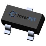 SMP4393TR
The activity of extra discounts on wholesale prices is in full swing…
Please fill in your contact information and we will send you the latest wholesale price list.






