 ChipApex | Global Electronic Components Supplier
SEARCH
Search Product
Search Post
— IC芯片 | 连接器 | 传感器 | 被动器件 —
Search productSearch post
— IC芯片 | 连接器 | 传感器 | 被动器件 —
Consult the customer manager about the wholesale price.
consultation hotline:86-132-6715-2157
email:[email protected]
Contact the product manager for consultation. One-stop consultation is available.
Do you want a lower wholesale price? Please send us your inquiry and we will reply immediately.
The SN74ALVC08PWR is a quadruple 2-input positive-AND gate from the Texas Instruments ALVC series, housed in a 14-pin TSSOP package. It operates within a supply voltage range of 1.65 V to 3.6 V and supports an operating temperature range of -40°C to +85°C. The device features a maximum propagation delay of 2.9 ns at 3.3 V and provides ±24 mA output drive capability. Input transition rise or fall rates are specified at 5 ns/V, with power dissipation capacitance per gate typically ranging from 24 pF to 26 pF.
Verify the specific ordering suffix matches the required tape-and-reel packaging configuration. Confirm that the moisture sensitivity level rating aligns with the assembly process capabilities. Ensure the lead finish specification meets the soldering requirements of the target printed circuit board design.
Select this component when multiple independent AND gates are required in a compact surface-mount form factor. Consider the ALVC series characteristics for applications demanding faster switching speeds compared to standard LVC devices while maintaining compatibility with lower supply voltages.
This part belongs to the SN74ALVC08 family of quadruple 2-input positive-AND gates. It shares functional specifications with variants such as SN74ALVC08DR and SN74ALVC08D, differing primarily in the physical package type. The PW suffix specifically denotes the Thin-Shrink Small-Outline Package (TSSOP) housing.
SN74ALVC08PWRE4
The maximum propagation delay is 2.9 ns when operating at a supply voltage of 3.3 V.
Yes, the absolute maximum ratings specify an input clamp current of -50 mA when the input voltage is less than 0 V.
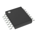 SN74ALVC08PWR
The activity of extra discounts on wholesale prices is in full swing…
Please fill in your contact information and we will send you the latest wholesale price list.





