 ChipApex | Global Electronic Components Supplier
SEARCH
Search Product
Search Post
— IC芯片 | 连接器 | 传感器 | 被动器件 —
Search productSearch post
— IC芯片 | 连接器 | 传感器 | 被动器件 —
Consult the customer manager about the wholesale price.
consultation hotline:86-132-6715-2157
email:[email protected]
Contact the product manager for consultation. One-stop consultation is available.
Do you want a lower wholesale price? Please send us your inquiry and we will reply immediately.
The SN74ALVC08PWRE4 is a quadruple 2-input positive-AND gate manufactured by Texas Instruments. It operates from a supply voltage range of 1.65 V to 3.6 V and features a maximum propagation delay of 2.9 ns at 3.3 V. The device provides ±24-mA output drive capability at 3.3 V and includes latch-up performance exceeding 250 mA per JESD 17. ESD protection exceeds 2000-V human-body model, 200-V machine model, and 1000-V charged-device model standards. It is housed in a 14-pin TSSOP (PW) package.
Verify the specific ordering suffix 'E4' indicates lead-free composition and RoHS compliance as defined in the manufacturer's documentation. Confirm the PW package designation corresponds to the TSSOP form factor. Ensure the operating temperature range aligns with system requirements, typically -40°C to +85°C for this part number. Cross-reference the datasheet revision date to ensure compatibility with latest design guidelines.
Select this component when multiple AND logic functions are required within a single integrated circuit. The ALVC series offers faster switching speeds compared to standard LVC counterparts while maintaining low power consumption. Consider the TSSOP package for surface-mount assembly where space constraints exist but larger footprints than SOT or QFN are acceptable. Verify input voltage levels match the target logic family thresholds.
This device belongs to the Texas Instruments SN74ALVC08 family of quadruple 2-input AND gates. It shares functional similarities with other members like the SN74ALVC08DR and SN74ALVC08D, differing primarily in packaging and reel specifications. The ALVC technology is designed for high-speed, low-power applications requiring operation across a wide voltage range.
SN74ALVC08PWR
The device performs the positive-AND function, represented by the equation Y = A · B.
No, the device is designed to operate from a supply voltage range of 1.65 V to 3.6 V.
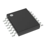 SN74ALVC08PWRE4
The activity of extra discounts on wholesale prices is in full swing…
Please fill in your contact information and we will send you the latest wholesale price list.





