 ChipApex | Global Electronic Components Supplier

SEARCH
Search Product
Search Post
— IC芯片 | 连接器 | 传感器 | 被动器件 —
Search productSearch post
— IC芯片 | 连接器 | 传感器 | 被动器件 —
Consult the customer manager about the wholesale price.
consultation hotline:86-132-6715-2157
email:[email protected]
Contact the product manager for consultation. One-stop consultation is available.
Do you want a lower wholesale price? Please send us your inquiry and we will reply immediately.
SN74ALVCH16269KR is listed in the Universal Bus Functions range at ChipApex. The manufacturer field lists Texas Instruments. Its product description is IC RGSTRD BUS EXCHANGER 56BGA. Review the specifications below when checking this part for your BOM.
The SN74ALVCH16269KR is a 12-bit to 24-bit registered bus exchanger with 3-state outputs, manufactured by Texas Instruments. It operates from a supply voltage range of 1.65 V to 3.6 V and features a maximum propagation delay of 5 ns at 3.3 V. The device provides ±24-mA output drive capability at 3.3 V and includes bus hold on data inputs to eliminate the need for external pullup or pulldown resistors. It is housed in a 56-pin VFBGA (GQL) package.
Verify the specific GQL package variant against the datasheet pinout diagram. Confirm that the application design accounts for the registered control terminals, as OE active states cannot be determined before the first clock pulse arrives during power-up sequences.
Select this component when a registered interface is required to bridge synchronous memory and processor buses. Ensure the system supports the 1.65-V to 3.6-V operating range and utilizes the 56-pin VFBGA footprint. Consider the registered nature of control signals when designing the clock distribution network.
This device belongs to the Texas Instruments Widebus family, which specializes in wide-data-path logic solutions. The SN74ALVCH16269KR specifically addresses bandwidth requirements by combining two 12-bit channels into a consolidated 24-bit interface while maintaining synchronization through internal registers.
No public confirmed substitute part numbers are available in the provided documentation.
The device incorporates active bus-hold circuitry on the data inputs, which holds unused or undriven inputs at a valid logic state, eliminating the need for external pullup or pulldown resistors.
Because the output enables (OE) are routed through a register, their active state cannot be determined before the arrival of the first clock pulse. A clock pulse should be applied as soon as possible after power-up to establish the state.
Explore related parts through Logic, Integrated Circuits (ICs), all product categories, ChipApex homepage.
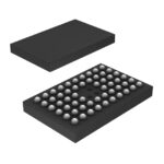 SN74ALVCH16269KR

The activity of extra discounts on wholesale prices is in full swing…
Please fill in your contact information and we will send you the latest wholesale price list.





