 ChipApex | Global Electronic Components Supplier
SEARCH
Search Product
Search Post
— IC芯片 | 连接器 | 传感器 | 被动器件 —
Search productSearch post
— IC芯片 | 连接器 | 传感器 | 被动器件 —
Consult the customer manager about the wholesale price.
consultation hotline:86-132-6715-2157
email:[email protected]
Contact the product manager for consultation. One-stop consultation is available.
Do you want a lower wholesale price? Please send us your inquiry and we will reply immediately.
The SN74AS808BN is a catalog logic device containing six independent 2-input AND drivers. It operates within a supply voltage range of 4.5 V to 5.5 V and supports an operating free-air temperature range from 0 °C to 70 °C. The component features a typical delay time of 3.2 ns with a capacitive load of 50 pF, while maintaining typical power dissipation below 13 mW per gate. It utilizes a standard plastic 300-mil DIP package with 20 pins.
Verify the specific ordering suffix 'N' corresponds to the standard plastic 300-mil PDIP package when sourcing components. Confirm that the required operating environment remains within the specified 0 °C to 70 °C temperature range. Ensure the system supply voltage strictly adheres to the 4.5 V to 5.5 V limits to maintain reliable operation and prevent damage to the internal circuitry.
Select this component for designs requiring multiple independent AND gates in a single integrated circuit. Consider its AS logic family characteristics for applications demanding faster switching speeds compared to standard TTL alternatives. Evaluate the 20-pin DIP footprint against available board space and routing constraints during the initial schematic capture phase.
This part belongs to the Texas Instruments 74AS (Advanced Schottky) logic family, which provides enhanced speed over standard variants. The SN74AS808BN represents the commercial-grade version of the SN54AS808B military device. It serves as a foundational building block for complex combinational logic networks in electronic systems.
SN74AS808BDW
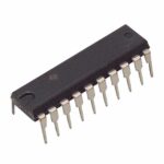 SN74AS808BN
The activity of extra discounts on wholesale prices is in full swing…
Please fill in your contact information and we will send you the latest wholesale price list.





