 ChipApex | Global Electronic Components Supplier
SEARCH
Search Product
Search Post
— IC芯片 | 连接器 | 传感器 | 被动器件 —
Search productSearch post
— IC芯片 | 连接器 | 传感器 | 被动器件 —
Consult the customer manager about the wholesale price.
consultation hotline:86-132-6715-2157
email:[email protected]
Contact the product manager for consultation. One-stop consultation is available.
Do you want a lower wholesale price? Please send us your inquiry and we will reply immediately.
The SN74BCT373DW is an octal transparent D-type latch with 3-state outputs manufactured by Texas Instruments. It operates within a supply voltage range of 4.5 V to 5.5 V and supports an operating temperature range of 0°C to 70°C. The device utilizes state-of-the-art BiCMOS design to reduce quiescent current. Key electrical characteristics include a low-level output current capability of up to 64 mA and a high-level output current of -15 mA at 5 V. Propagation delays from data inputs (D) to outputs (Q) are typically 6.7 ns for low-to-high transitions and 5.9 ns for high-to-low transitions.
Verify the specific ordering suffix 'DW' corresponds to the SOIC package type and tube packing configuration as listed in the official ordering information. Confirm that the required operating temperature range aligns with the commercial grade specifications (0°C to 70°C). Ensure compatibility with the 4.5 V to 5.5 V supply voltage requirements before procurement.
Select this component when designing systems requiring octal data storage with bus-compatible three-state outputs. The BiCMOS technology offers lower power consumption compared to standard bipolar designs. Consider the 64 mA low-level drive strength for applications involving heavy capacitive loading on shared bus lines.
This part belongs to the SN74BCT series, which features BiCMOS technology designed to combine the speed of bipolar circuits with the low power consumption of CMOS. The SN74BCT373 specifically provides eight independent latches with tri-state control, distinguishing it from non-latching buffers or single-bit flip-flops within the broader logic IC family.
SN74BCT373N (PDIP package)
The OE input only controls the external output state. It does not affect the internal operations of the latches; old data can be retained or new data entered while outputs are in the high-impedance state.
To ensure the high-impedance state during power up or power down, the OE pin should be tied to VCC through a pullup resistor.
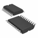 SN74BCT373DW
The activity of extra discounts on wholesale prices is in full swing…
Please fill in your contact information and we will send you the latest wholesale price list.






