 ChipApex | Global Electronic Components Supplier
SEARCH
Search Product
Search Post
— IC芯片 | 连接器 | 传感器 | 被动器件 —
Search productSearch post
— IC芯片 | 连接器 | 传感器 | 被动器件 —
Consult the customer manager about the wholesale price.
consultation hotline:86-132-6715-2157
email:[email protected]
Contact the product manager for consultation. One-stop consultation is available.
Do you want a lower wholesale price? Please send us your inquiry and we will reply immediately.
The SN74GTL16616DGGR is a 17-bit Universal Bus Transceiver (UBT) from the Widebus family, translating between LVTTL and GTL/GTL+ signal levels. It operates with VCC(3.3V) for LVTTL buffers and VCC(5V) for internal/GTL circuitry. The device supports mixed-mode operation on the A-port and control inputs, featuring buffered clock outputs (CLKOUT/CLKIN). It provides transparent, latched, clocked, or clock-enabled data transfer modes. Operating temperature range is -40°C to +85°C.
Verify the specific ordering suffix DGGR corresponds to the TSSOP-56 tape and reel package configuration. Confirm that the design accommodates the dual supply voltage requirements of 3.3V and 5V as specified in the recommended operating conditions. Ensure proper termination voltages (VTT) and reference voltages (VREF) are established for the intended GTL or GTL+ signal level operation.
Select this component when a 17-bit transceiver is required to bridge LVTTL and GTL/GTL+ domains with flexible timing control. The UBT architecture allows for complex data handling modes beyond simple buffering. Consider the distributed VCC and GND pins for noise minimization in high-speed switching environments. Verify compatibility with existing clock distribution networks due to the dedicated CLKOUT and CLKIN functions.
This device belongs to Texas Instruments' Widebus family, designed for high-performance bus interfacing. It serves as an equivalent to the '16601 function but with enhanced GTL/GTL+ support. The SN74GTL16616 series addresses the need for reliable data translation in mixed-voltage systems, providing robust ESD protection and latch-up performance exceeding standard class II ratings.
SN74GTL16616DL
Active bus-hold circuitry holds unused or undriven LVTTL inputs at a valid logic state, eliminating the need for external pullup or pulldown resistors.
The CLKOUT pin provides a copy of the CLKAB signal at GTL/GTL+ signal levels, allowing for buffered clock distribution within the GTL domain.
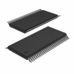 SN74GTL16616DGGR
The activity of extra discounts on wholesale prices is in full swing…
Please fill in your contact information and we will send you the latest wholesale price list.





