 ChipApex | Global Electronic Components Supplier

SEARCH
Search Product
Search Post
— IC芯片 | 连接器 | 传感器 | 被动器件 —
Search productSearch post
— IC芯片 | 连接器 | 传感器 | 被动器件 —
Consult the customer manager about the wholesale price.
consultation hotline:86-132-6715-2157
email:[email protected]
Contact the product manager for consultation. One-stop consultation is available.
Do you want a lower wholesale price? Please send us your inquiry and we will reply immediately.
SN74GTLP817DGVR is listed in the Translators, Level Shifters range at ChipApex. The manufacturer field lists Texas Instruments. Its product description is IC TRANSLATOR BIDIR 24TVSOP. Review the specifications below when checking this part for your BOM.
The SN74GTLP817DGVR is a fanout driver providing LVTTL-to-GTLP and GTLP-to-LVTTL signal-level translation. It operates at VCC = 3.3V with VTT = 1.5V and VREF = 1V for GTLP levels. The device features a 1-to-2 LVTTL-to-GTLP driver (AO to BO) and a 1-to-6 GTLP-to-LVTTL driver (BI to AO). Propagation delays range from 1.5ns to 6.3ns depending on edge rate control. Outputs support medium drive (50mA) for GTLP and reduced drive (±12mA) for LVTTL.
Verify the package type matches the required footprint, as the SN74GTLP817 family includes SOIC, TSSOP, and TVSOP options. Confirm that the specific DGVR suffix corresponds to the TVSOP package variant needed for your design. Ensure compatibility with the 3.3V supply voltage and GTLP termination requirements before finalizing procurement.
Select this component when bidirectional translation between LVTTL and GTLP is required in a single package. Consider the variable edge-rate control feature if optimizing data-transfer rates and signal integrity for distributed backplane loads is critical. Verify that the medium-drive capability meets the impedance requirements of the target bus architecture.
This part belongs to the SN74GTLP series of fanout drivers designed by Texas Instruments. It utilizes OEC circuitry to minimize bus settling time and improve signal integrity. The device supports both GTL and GTLP signal levels, offering flexibility in system design while maintaining compatibility with standard TTL and 5-V CMOS inputs on the LVTTL side.
SN74GTLP817DW
The Edge-Rate Control (ERC) input adjusts the B-port output rise and fall times. Connecting it to VCC selects slow edge rates, while connecting it to GND selects fast edge rates, allowing optimization for data-transfer rate and signal integrity.
The device includes Ioff circuitry to disable outputs and prevent backflow current when powered down, and power-up 3-state circuitry to place outputs in a high-impedance state during power transitions, preventing driver conflicts.
Explore related parts through Logic, Integrated Circuits (ICs), all product categories, ChipApex homepage.
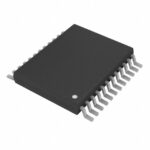 SN74GTLP817DGVR

The activity of extra discounts on wholesale prices is in full swing…
Please fill in your contact information and we will send you the latest wholesale price list.





