ChipApex | Global Electronic Components Supplier
SEARCH
Search Product
Search Post
— IC芯片 | 连接器 | 传感器 | 被动器件 —
Search productSearch post
— IC芯片 | 连接器 | 传感器 | 被动器件 —
Consult the customer manager about the wholesale price.
consultation hotline:86-132-6715-2157
email:[email protected]
Contact the product manager for consultation. One-stop consultation is available.
Do you want a lower wholesale price? Please send us your inquiry and we will reply immediately.
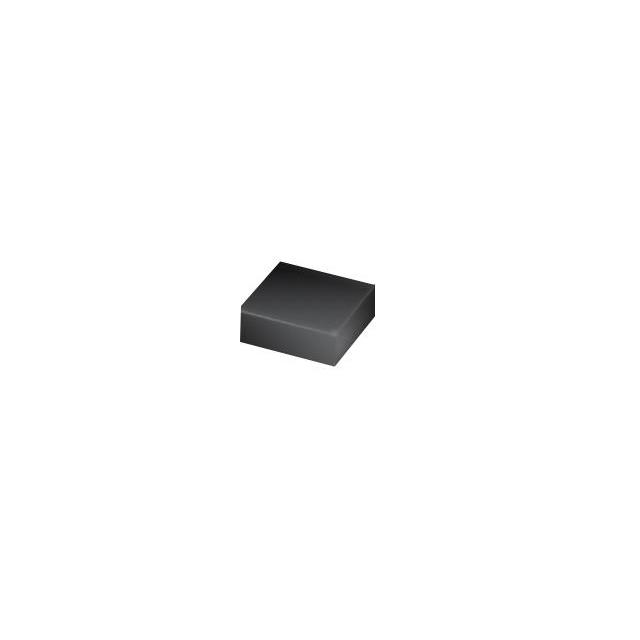
The SSFB12N05 is a complementary N-channel and P-channel MOSFET in a DFN2x2-6L 2EP package. The N-channel device offers a drain-source voltage of 12V, continuous current of 5A at 25°C, and maximum on-resistance of 32mΩ at VGS=4.5V. The P-channel counterpart provides -12V breakdown, -5A continuous current, and 74mΩ maximum on-resistance at VGS=-4.5V. Both channels support a junction temperature range of -55 to +150°C.
Verify the specific ordering code against the manufacturer's official documentation to ensure correct component revision. Confirm that the DFN2x2-6L 2EP footprint matches your PCB layout requirements. Check for any RoHS or REACH compliance statements in the latest datasheet version before finalizing procurement specifications.
Select this component when space-constrained designs require both N-channel and P-channel switching capabilities. The low thermal resistance and small outline make it suitable for applications where heat dissipation is limited by board area. Ensure gate drive voltages align with the specified thresholds for optimal RDS(on) performance.
This dual MOSFET integrates separate N-channel and P-channel structures into one unit. It utilizes advanced processing techniques to achieve high cell density. The design focuses on minimizing on-resistance while maintaining fast switching speeds. This integration reduces component count compared to using discrete devices.
No public confirmed substitute part numbers are available.
 SSFB12N05
The activity of extra discounts on wholesale prices is in full swing…
Please fill in your contact information and we will send you the latest wholesale price list.