 ChipApex | Global Electronic Components Supplier
SEARCH
Search Product
Search Post
— IC芯片 | 连接器 | 传感器 | 被动器件 —
Search productSearch post
— IC芯片 | 连接器 | 传感器 | 被动器件 —
Consult the customer manager about the wholesale price.
consultation hotline:86-132-6715-2157
email:[email protected]
Contact the product manager for consultation. One-stop consultation is available.
Do you want a lower wholesale price? Please send us your inquiry and we will reply immediately.
The SSM6322ACPZ-RL is a dual-channel audio amplifier from Analog Devices, housed in a 24-lead LFCSP package. It operates on a supply voltage ranging from ±3.3 V to ±6 V. The device delivers high output current drive capability, exceeding 100 mA rms into heavy loads such as 16 Ω or 32 Ω impedances. Key performance metrics include a gain bandwidth of 25 MHz and a slew rate of 18 V/μs at ±5 V. Distortion is minimized with THD+N reaching -121 dB at 1 kHz with a 2 V rms output into a 32 Ω load. Noise performance features an A-weighted output noise of 1.8 μV rms across the 10 Hz to 22 kHz band.
Verify the specific ordering suffix RL against the manufacturer's official documentation to confirm reel packaging specifications. Ensure compatibility with the required LFCSP-24 footprint and thermal pad connection requirements during procurement planning. Cross-reference the component revision history to validate the manufacturing date code and ensure it meets project lifecycle requirements.
Select this component when designing systems requiring high dynamic range and low distortion for portable audio applications. The integrated solution reduces external component count compared to discrete implementations. Consider the ±3.3 V to ±6 V operating range and the specific shutdown pin configurations for power management strategies in battery-operated devices.
This part belongs to the SSM6322 series of integrated stereo audio amplifiers manufactured by Analog Devices Inc. It utilizes a proprietary XFCB process technology designed for exceptionally low 1/f noise and high load drive capabilities. The device combines a difference amplifier configuration with a common-mode loop to maximize audio fidelity while minimizing power dissipation.
Consult the official datasheet ordering guide for confirmed substitute part numbers. Verify pinout compatibility and electrical specifications before substituting any alternative components.
The device features an internal common-mode loop that sets the input terminals to a DC voltage defined by the REF pins, ensuring the DAC source resistors have equal voltage drops for optimal distortion performance.
SD controls the output buffer shutdown while keeping the input stage active, whereas SD2 shuts down the entire device, reducing quiescent current to approximately 15 μA.
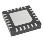 SSM6322ACPZ-RL
The activity of extra discounts on wholesale prices is in full swing…
Please fill in your contact information and we will send you the latest wholesale price list.





