 ChipApex | Global Electronic Components Supplier
SEARCH
Search Product
Search Post
— IC芯片 | 连接器 | 传感器 | 被动器件 —
Search productSearch post
— IC芯片 | 连接器 | 传感器 | 被动器件 —
Consult the customer manager about the wholesale price.
consultation hotline:86-132-6715-2157
email:[email protected]
Contact the product manager for consultation. One-stop consultation is available.
Do you want a lower wholesale price? Please send us your inquiry and we will reply immediately.
The SSM6L12TU,LF is a dual-channel silicon MOSFET from Toshiba's U-MOSIII series, featuring one N-channel and one P-channel transistor in a UF-6 package. The N-channel Q1 provides a drain-source breakdown voltage of 30 V with a maximum on-resistance of 180 mΩ at VGS = 2.5 V. The P-channel Q2 offers a breakdown voltage of -20 V and a maximum on-resistance of 430 mΩ at VGS = -2.5 V. Both channels support a continuous drain current of ±0.5 A and operate within an ambient temperature range of -55°C to +150°C.
Verify the component against official Toshiba datasheets to confirm pinout alignment and electrical ratings match your design requirements. Ensure that thermal management strategies account for the specified power dissipation limits on standard FR4 boards. Confirm compliance with relevant environmental directives such as RoHS before finalizing procurement specifications.
Select this component when space constraints require a dual-channel configuration in a compact UF-6 footprint. It is appropriate for designs needing matched N/P channel pairs with distinct voltage ratings of 30 V and -20 V. Consider the specific gate threshold voltages and on-resistance values at your operating gate drive levels to ensure proper switching performance.
This device belongs to Toshiba's U-MOSIII family of silicon MOSFETs designed for general-purpose switching. The SSM6L12TU integrates complementary N-channel and P-channel transistors into a single package, facilitating simplified circuit layouts for bridge drivers or logic-level interfaces while maintaining low profile and weight characteristics.
Consult Toshiba documentation for direct equivalents within the SSM6L series. Verify that any substitute maintains compatible UF-6 packaging, voltage ratings, and thermal characteristics to ensure seamless integration without redesigning the PCB layout or cooling infrastructure.
The N-channel (Q1) has a maximum rating of 30 V, while the P-channel (Q2) has a maximum rating of -20 V.
For Q1, RDS(ON) is maximized at 180 mΩ when VGS is 2.5 V, and for Q2, it is maximized at 430 mΩ when VGS is -2.5 V.
No, the datasheet explicitly restricts use in unintended applications like automotive safety devices unless specifically permitted.
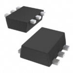 SSM6L12TU,LF
The activity of extra discounts on wholesale prices is in full swing…
Please fill in your contact information and we will send you the latest wholesale price list.





