ChipApex | Global Electronic Components Supplier
SEARCH
Search Product
Search Post
— IC芯片 | 连接器 | 传感器 | 被动器件 —
Search productSearch post
— IC芯片 | 连接器 | 传感器 | 被动器件 —
Consult the customer manager about the wholesale price.
consultation hotline:86-132-6715-2157
email:[email protected]
Contact the product manager for consultation. One-stop consultation is available.
Do you want a lower wholesale price? Please send us your inquiry and we will reply immediately.
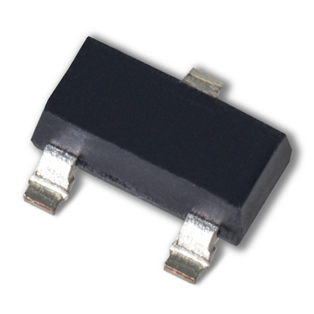
The SST112 is a single N-channel Junction Field-Effect Transistor (JFET) switch manufactured by Linear Integrated Systems in the SOT-23 surface-mount package. It serves as a direct replacement for the Siliconix J/SST111 series. Key electrical characteristics include a gate-to-source cutoff voltage (VGS(off)) ranging from -1V to -5V, a drain-to-source saturation current (IDSS) of 2mA, and a typical on-resistance (rDS(on)) of 50Ω. The device features low gate leakage current of 5pA and fast switching capabilities with turn-on times around 2ns. It operates within a junction temperature range of -55°C to +150°C.
Verify the specific VGS(off) bin (-1V to -5V) required for your circuit design, as this parameter varies significantly between devices in the same family. Confirm that the SOT-23 package dimensions match your PCB footprint. Ensure the operating conditions do not exceed the continuous power dissipation limits, particularly at elevated ambient temperatures where derating applies.
Select the SST112 when a low on-resistance of 50Ω and moderate saturation current of 2mA are acceptable. Compare against the SST111 if lower resistance (30Ω) is needed, or the SST113 if higher resistance (100Ω) suits the application. Consider the input capacitance of 12pF for high-frequency signal integrity requirements. Verify that the -35V breakdown voltage meets the system's maximum voltage constraints.
This component belongs to the J/SST111 series of single N-channel JFET switches produced by Linear Integrated Systems. The company utilizes proprietary processes originally developed at Amelco, Union Carbide, Intersil, and Micro Power Systems. The SST112 variant specifically targets applications requiring a balance between low on-resistance and manageable gate leakage, housed in the compact SOT-23 form factor alongside the TO-92 J-series equivalent.
The datasheet explicitly identifies this part as a direct replacement for the Siliconix J/SST111 series. When substituting, ensure the replacement device matches the required VGS(off) range and rDS(on) specifications. Cross-reference pinouts carefully, as the SOT-23 pin configuration (Drain, Gate, Source) must align with the original design intent.
The typical turn-on time (td(on)) is 2 nanoseconds under test conditions of VDD = 10V and VGS(H) = 0V.
The SST112 has a typical on-resistance (rDS(on)) of 50Ω, whereas the SST111 typically features a lower on-resistance of 30Ω.
The absolute maximum gate-to-source voltage (BVGSS) is rated at -35V.
 SST112 SOT-23 3L ROHS
The activity of extra discounts on wholesale prices is in full swing…
Please fill in your contact information and we will send you the latest wholesale price list.