 ChipApex | Global Electronic Components Supplier

SEARCH
Search Product
Search Post
— IC芯片 | 连接器 | 传感器 | 被动器件 —
Search productSearch post
— IC芯片 | 连接器 | 传感器 | 被动器件 —
Consult the customer manager about the wholesale price.
consultation hotline:86-132-6715-2157
email:[email protected]
Contact the product manager for consultation. One-stop consultation is available.
Do you want a lower wholesale price? Please send us your inquiry and we will reply immediately.
SY89464UMY is listed in the Clock Buffers, Drivers range at ChipApex. The manufacturer field lists Microchip Technology. Its product description is IC CLK MULTIPLX 2:10 2GHZ 44MLF. Review the specifications below when checking this part for your BOM.
The SY89464UMY is a low jitter LVPECL fanout buffer featuring a 2:1 differential input multiplexer with Runt Pulse Eliminator (RPE) and Fail-Safe Input (FSI). It provides ten precision LVPECL outputs from two differential inputs. The device operates on a 2.5V ±5% or 3.3V ±10% supply, supporting frequencies up to 2.0 GHz. Key electrical parameters include propagation delays under 1100ps, rise/fall times below 220ps, and jitter specifications of less than 1ps RMS random and cycle-to-cycle jitter. It functions within an industrial temperature range of -40°C to +85°C.
Verify the package marking matches the part number exactly. Confirm the lead finish is Matte-Sn Pb-Free. Ensure the operating range corresponds to the Industrial specification (-40°C to +85°C). Check that the ordering suffix indicates the correct tape and reel quantity if applicable.
Select this component when redundant clock switching without runt pulses is required. Ensure the input signal amplitude meets the minimum 100mV single-ended requirement. Verify compatibility with 2.5V or 3.3V power supplies. Consider the 44-pin QFN package constraints for thermal management and PCB layout.
This device belongs to Micrel’s Precision Edge product line, designed for high-speed applications. It is manufactured by Micrel, Inc., which was acquired by Microchip Technology. The part is optimized for telecom and enterprise server environments requiring precise clock distribution.
SY89465UMY: Similar function but uses LVDS outputs instead of LVPECL.
The RPE circuit ensures glitchless switchover between two clocks by preventing short cycles or runt pulses during the transition, utilizing a three-stage process for seamless switching.
The CAP pin controls the Power-On Reset delay. Connecting it to VCC disables the RPE function, while connecting a capacitor allows the internal RPE logic to start up in a known state.
Yes, the unique internal termination architecture allows the device to interface with both AC- and DC-coupled differential signals without external level shifting or termination networks.
Explore related parts through Clock/Timing, Integrated Circuits (ICs), all product categories, ChipApex homepage.
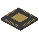 SY89464UMY

The activity of extra discounts on wholesale prices is in full swing…
Please fill in your contact information and we will send you the latest wholesale price list.






