 ChipApex | Global Electronic Components Supplier

SEARCH
Search Product
Search Post
— IC芯片 | 连接器 | 传感器 | 被动器件 —
Search productSearch post
— IC芯片 | 连接器 | 传感器 | 被动器件 —
Consult the customer manager about the wholesale price.
consultation hotline:86-132-6715-2157
email:[email protected]
Contact the product manager for consultation. One-stop consultation is available.
Do you want a lower wholesale price? Please send us your inquiry and we will reply immediately.
SY89809LTH-TR is listed in the Clock Buffers, Drivers range at ChipApex. The manufacturer field lists Microchip Technology. Its product description is IC CLK BUFFER 2:9 500MHZ 32TQFP. Review the specifications below when checking this part for your BOM.
The SY89809LTH-TR is a high-performance bus clock driver manufactured by Microchip Technology, housed in a 32-pin TQFP package. It provides nine differential HSTL output pairs and supports both HSTL and LVPECL inputs selected via the CLK_SEL pin. The device operates with a 3.3V core supply (VCCI: 3.0V to 3.6V) and an 1.8V output supply (VCCO: 1.6V to 2.0V). Key electrical parameters include a maximum operating frequency of 500MHz, a maximum part-to-part skew of 200ps, and a maximum pin-to-pin skew of 50ps. The synchronous Output Enable (OE) prevents runt clock pulses.
Verify component authenticity through authorized channels as the datasheet indicates the product is not recommended for new designs. Confirm lead finish specifications, as the TH suffix denotes a Pb-Free package with NiPdAu finish. Ensure compliance with RoHS standards and check moisture sensitivity level (MSL 3) requirements for surface mount assembly processes.
Select this component when a large number of precisely aligned clock signals are required from a single source. Ensure the design accommodates separate 3.3V and 1.8V power supplies for the core and output buffers respectively. Verify that the input signal matches either HSTL or LVPECL standards, as the device does not support simultaneous operation of both input types.
The SY89809L belongs to the Precision Edge series of clock drivers originally developed by Micrel, which was subsequently acquired by Microchip Technology. The device is designed to replace standard clock distribution solutions requiring ultra-low skew across multiple outputs. The -TR suffix indicates the component is supplied in tape and reel packaging for automated surface-mount assembly.
The datasheet explicitly states the SY89809L is not recommended for new designs. Engineers should evaluate newer generation clock buffer families from Microchip or other manufacturers that offer similar 1:9 fanout ratios with updated process technologies and improved power efficiency.
The input source is selected via the CLK_SEL pin. When CLK_SEL is LOW, the HSTL_CLK inputs are active. When CLK_SEL is HIGH, the LVPECL_CLK inputs are active.
The OE signal synchronizes the enabling and disabling of outputs with the low level of the clock signal. This ensures outputs are disabled only when already in the LOW state, preventing the generation of runt clock pulses.
The device requires two distinct power supplies: VCCI (Core Power) must be between 3.0V and 3.6V, and VCCO (Output Buffer Power) must be between 1.6V and 2.0V.
Explore related parts through Clock/Timing, Integrated Circuits (ICs), all product categories, ChipApex homepage.
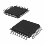 SY89809LTH-TR

The activity of extra discounts on wholesale prices is in full swing…
Please fill in your contact information and we will send you the latest wholesale price list.





