 ChipApex | Global Electronic Components Supplier
SEARCH
Search Product
Search Post
— IC芯片 | 连接器 | 传感器 | 被动器件 —
Search productSearch post
— IC芯片 | 连接器 | 传感器 | 被动器件 —
Consult the customer manager about the wholesale price.
consultation hotline:86-132-6715-2157
email:[email protected]
Contact the product manager for consultation. One-stop consultation is available.
Do you want a lower wholesale price? Please send us your inquiry and we will reply immediately.
The TC74LCX573FK(EL,K) is a low-voltage octal D-type latch manufactured by Toshiba Semiconductor and Storage. It operates within a supply voltage range of 1.65 V to 3.6 V, with specific data retention support down to 1.5 V. The device features 5-V tolerant inputs and outputs, allowing interface with 5-V environments. Propagation delay (D-Q) is 8.0 ns maximum at 3.0–3.6 V. Output drive current reaches 24 mA minimum at 3.0 V. Quiescent supply current is 10 µA maximum. Input leakage current is ±5 µA. Operating temperature spans -40 °C to 85 °C.
Verify the specific package variant required, as the FK suffix denotes VSSOP packaging while F denotes SOP. Confirm manufacturing date codes if 1.8 V operation is critical, as electrical characteristics for this voltage apply only to units produced from January 2009 onward. Ensure compliance with RoHS directives and check for any export control classifications relevant to the destination region before finalizing orders.
Select this component when an octal latch with 5-V tolerance is needed for 3.3-V systems. It is suitable for designs requiring CMOS low power dissipation alongside high-speed performance. Consider the VSSOP package for space-constrained surface-mount applications. Verify that the input rise/fall times remain within the specified 10 ns/V limit to ensure proper timing margins.
This part belongs to the TC74LCX series of low-voltage CMOS logic devices. It functions as an octal D-type latch, distinct from flip-flops by its level-sensitive latch enable mechanism rather than edge-triggered clocking. The device is designed for general-purpose digital logic applications where data latching and bus isolation are required.
Direct substitutes include the TC74LCX573F (SOP package). Other compatible parts within the 74LCX family may offer similar functionality but require verification of package dimensions and exact electrical parameters against the datasheet specifications.
Yes, but the specific electrical characteristics for VCC = 1.8 ± 0.15 V apply only to products manufactured from January 2009 onward.
When the LE input is high, the outputs follow the D inputs. When LE goes low, the Q outputs are latched at the value present at the D inputs at that moment.
When the OE input is high, the eight outputs enter a high-impedance state, effectively disconnecting them from the circuit.
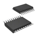 TC74LCX573FK(EL,K)
The activity of extra discounts on wholesale prices is in full swing…
Please fill in your contact information and we will send you the latest wholesale price list.






