 ChipApex | Global Electronic Components Supplier
SEARCH
Search Product
Search Post
— IC芯片 | 连接器 | 传感器 | 被动器件 —
Search productSearch post
— IC芯片 | 连接器 | 传感器 | 被动器件 —
Consult the customer manager about the wholesale price.
consultation hotline:86-132-6715-2157
email:[email protected]
Contact the product manager for consultation. One-stop consultation is available.
Do you want a lower wholesale price? Please send us your inquiry and we will reply immediately.
The TDA8510J is a Class-B power amplifier integrated circuit designed for multimedia and active speaker systems. It integrates one 26 W Bridge-Tied Load (BTL) channel and two 13 W Single-Ended (SE) channels within a single 17-lead DBS17P package. The device operates on a supply voltage ranging from 6 V to 18 V, delivering high output power with low quiescent current of 80 mA typical. It features fixed gains of 26 dB for the BTL channel and 20 dB for SE channels, ensuring straightforward integration into audio designs requiring robust amplification capabilities.
Verify component authenticity through authorized NXP distributors as this part may be discontinued. Confirm package integrity and lead condition upon receipt. Ensure storage conditions adhere to specified limits to prevent degradation. Cross-reference ordering information with official manufacturer documentation to validate specific suffix variations before procurement.
Select this amplifier for applications requiring combined BTL and SE outputs in a compact form factor. Evaluate thermal management requirements based on the specified junction-to-case resistance. Consider the fixed gain structure when designing input stages. Ensure supply voltage stability within the 6 V to 18 V range to maintain optimal ripple rejection and output performance.
The TDA8510J belongs to the Philips Semiconductors (now NXP) family of Class-B power amplifiers. It was originally released as a preliminary specification in December 1999. The device represents a solution for multi-channel audio amplification where space constraints necessitate integrating multiple amplifier channels into a single package with extensive built-in protection features.
Consult official NXP documentation for confirmed substitute part numbers. Verify pin compatibility and electrical specifications against the original design requirements before implementing any alternative components.
During a short-circuit to ground or supply, the output stages switch off for approximately 20 ms. The diagnostic pin remains LOW during this period. After 20 ms, it checks for the fault presence for 50 μs, resulting in a low average current consumption while maintaining protection.
To prevent switch-on plops, keep the amplifier in mute mode for at least 100 ms after power-up. This allows sufficient time for the input capacitors at pins 1, 3, 15, and 17 to charge fully before enabling the audio signal path.
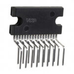 TDA8510J/N2,112
The activity of extra discounts on wholesale prices is in full swing…
Please fill in your contact information and we will send you the latest wholesale price list.







