 ChipApex | Global Electronic Components Supplier
SEARCH
Search Product
Search Post
— IC芯片 | 连接器 | 传感器 | 被动器件 —
Search productSearch post
— IC芯片 | 连接器 | 传感器 | 被动器件 —
Consult the customer manager about the wholesale price.
consultation hotline:86-132-6715-2157
email:[email protected]
Contact the product manager for consultation. One-stop consultation is available.
Do you want a lower wholesale price? Please send us your inquiry and we will reply immediately.
The THCV220-B is a receiver LSI designed to convert V-by-One HS input signals into 32-bit LVCMOS output signals. It supports a maximum effective data rate of 3.0 Gbps per lane, enabling the reception of 720p/60Hz video with 30-bit color depth. The device operates on a supply voltage range of 2.5V to 3.3V and is housed in a QFN64 package. It features AEC-Q100 compliance and integrated ESD protection, ensuring reliability for automotive applications.
Verify the specific suffix B against official THine Solutions documentation to confirm exact electrical or mechanical variations. Ensure compatibility with recommended transmitter models such as the THCV219 or THCV233 for signal integrity. Confirm RoHS status and packaging details directly from the manufacturer's current datasheet before procurement.
Select this component when a single-lane V-by-One HS source must drive a 32-bit parallel interface. Verify that the target LCD controller accepts LVCMOS levels within the 2.5V to 3.3V range. Consider the thermal performance of the QFN64 package if operating near the upper limit of the -40°C to 85°C temperature range.
This part belongs to the THine Solutions V-by-One HS family of display interface transceivers. It serves as the receiving end counterpart to transmitters like the THCV219. The series addresses the bandwidth requirements for high-resolution automotive displays while maintaining low power consumption and robust signal transmission over short cable runs.
Publicly confirmed substitute part numbers are not available in the provided documentation. Direct replacement requires matching the V-by-One HS protocol, 32-bit LVCMOS output width, and QFN64 footprint. Consult THine Solutions for any updated revisions or alternative devices within the same product line.
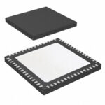 THCV220-B
The activity of extra discounts on wholesale prices is in full swing…
Please fill in your contact information and we will send you the latest wholesale price list.





