 ChipApex | Global Electronic Components Supplier
SEARCH
Search Product
Search Post
— IC芯片 | 连接器 | 传感器 | 被动器件 —
Search productSearch post
— IC芯片 | 连接器 | 传感器 | 被动器件 —
Consult the customer manager about the wholesale price.
consultation hotline:86-132-6715-2157
email:[email protected]
Contact the product manager for consultation. One-stop consultation is available.
Do you want a lower wholesale price? Please send us your inquiry and we will reply immediately.
The TLC976CDGG is a multichip module (MCM) subsystem designed for Charge-Coupled Device (CCD) signal processing. It integrates a correlated double sampler (CDS), automatic gain control (AGC), black level clamp circuit, and a 10-bit analog-to-digital converter (ADC). The device operates with a 5-V analog supply and a 3.3-V digital supply. Key electrical parameters include a maximum conversion rate of 20 MSPS, an AGC gain range of 5 dB to 39 dB, and differential nonlinearity of 0.75 LSB typical. It utilizes a 56-pin TSSOP package.
Verify the obsolete status of the TLC976CDGG before design implementation. Confirm that the 56-pin TSSOP package dimensions align with current PCB layout constraints. Ensure power supply decoupling meets the specified requirements for the separate analog and digital domains to maintain signal integrity.
Select this component when interfacing directly with CCD sensors requiring integrated signal conditioning. The MCM architecture reduces substrate noise compared to discrete solutions. Verify compatibility with 3.3-V CMOS digital interfaces and ensure the 5-V analog supply is available within the recommended operating conditions.
The TLC976CDGG belongs to the Texas Instruments TLC976 family of CCD signal processors. It combines multiple functions into a single compact package, replacing larger discrete configurations such as two separate 32-pin QFPs. The DGG suffix indicates the 56-pin TSSOP plastic small-outline package with a 0.50 mm pin pitch.
The product is listed as obsolete. No specific replacement part numbers are documented in the provided source material. Designers should consult Texas Instruments for current alternatives or evaluate third-party compatible devices.
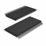 TLC976CDGG
The activity of extra discounts on wholesale prices is in full swing…
Please fill in your contact information and we will send you the latest wholesale price list.





