 ChipApex | Global Electronic Components Supplier
SEARCH
Search Product
Search Post
— IC芯片 | 连接器 | 传感器 | 被动器件 —
Search productSearch post
— IC芯片 | 连接器 | 传感器 | 被动器件 —
Consult the customer manager about the wholesale price.
consultation hotline:86-132-6715-2157
email:[email protected]
Contact the product manager for consultation. One-stop consultation is available.
Do you want a lower wholesale price? Please send us your inquiry and we will reply immediately.
The TLV987CPFB is a monolithic analog signal processor and digitizer designed for area CCD sensor interfacing in digital camera applications. It integrates input clamp circuitry, a correlated double sampler (CDS), and a programmable gain amplifier (PGA) with a 0-dB to 36-dB range. The device features a 10-bit ADC operating at 27 MSPS, two internal DACs for offset calibration, and two user DACs. It operates from a single 3-V analog supply and a 1.8-V to 4.4-V digital interface supply, consuming 200 mW typically. The component is housed in a 48-pin TQFP package.
Verify the specific suffix CPFB corresponds to the commercial temperature range (0°C to 70°C) and TQFP package as documented in the SLAS211A datasheet. Confirm that production data reflects current manufacturing status, as older components may have limited availability or require obsolescence checks.
Select this component when interfacing area CCD sensors requiring integrated signal conditioning and digitization. Ensure the system supports a single 3-V analog supply and a separate 1.8-V to 4.4-V digital I/O supply. Verify that the 27 MSPS throughput and 10-bit resolution meet the image quality requirements.
The TLV987 is part of Texas Instruments' specialized CCD sensor signal processor family. It consolidates multiple discrete analog functions into a single CMOS IC, reducing board space and complexity for consumer imaging devices. The CPFB variant denotes the commercial grade version in the 48-lead thin quad flatpack package.
No public confirmed substitute part numbers are available in the provided documentation. Designers should evaluate functional equivalents based on pin compatibility and signal chain specifications if the TLV987 is no longer in production.
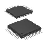 TLV987CPFB
The activity of extra discounts on wholesale prices is in full swing…
Please fill in your contact information and we will send you the latest wholesale price list.





