 ChipApex | Global Electronic Components Supplier

SEARCH
Search Product
Search Post
— IC芯片 | 连接器 | 传感器 | 被动器件 —
Search productSearch post
— IC芯片 | 连接器 | 传感器 | 被动器件 —
Consult the customer manager about the wholesale price.
consultation hotline:86-132-6715-2157
email:[email protected]
Contact the product manager for consultation. One-stop consultation is available.
Do you want a lower wholesale price? Please send us your inquiry and we will reply immediately.
TMS320DM642AZDK6 is listed in the Digital Signal Processor Dsp range at ChipApex. The manufacturer field lists Texas Instruments. Its product description is IC FIXED-POINT DSP 548-FCBGA. Review the specifications below when checking this part for your BOM.
The TMS320DM642AZDK6 is a video and imaging fixed-point digital signal processor based on the C64x+ DSP core. It operates at clock rates of 500, 600, or 720 MHz, delivering up to 5760 MIPS. The architecture features eight independent functional units (two multipliers and six ALUs) supporting VelociTI.2 extensions for parallel processing. On-chip memory includes 16 KB L1P cache, 16 KB L1D cache, and 256 KB configurable L2 RAM/cache. Key peripherals include three configurable video ports, a 10/100 Mb/s Ethernet MAC, McASP0, PCI, and EMIF. The device utilizes a 548-pin BGA package with 0.8-mm ball pitch.
Verify the specific speed grade suffix (-500, -600, or -720) required for the target application frequency. Confirm that the ZDK suffix corresponds to the correct 548-pin BGA package with 0.8-mm ball pitch. Ensure compatibility with existing development tools such as Code Composer Studio for software integration.
Select the appropriate clock speed variant based on computational requirements. The DM642 supports both little-endian and big-endian modes. Developers must account for peripheral pin multiplexing, as certain interfaces like VP0 share pins with McBSP0 and McASP0 control lines. Verify power supply requirements, noting the 1.2V or 1.4V core voltage depending on the speed grade.
The TMS320DM642 belongs to the TI C6000 DSP platform, specifically designed for high-performance digital media applications. It is code-compatible with other C64x devices. The AZDK6 designation indicates a specific manufacturing lot or revision within the standard production data set for this video-focused processor family.
Direct replacements within the same package and pinout are limited due to the age of the component. Consider the TMS320DM643 for similar functionality with potential performance variations, or newer DaVinci processors for updated feature sets, though these may require schematic and software redesigns.
At a clock rate of 720 MHz, the device achieves a peak performance of 5760 million instructions per second (MIPS).
The 2-Mbit (256-KByte) L2 memory can be configured as fully mapped RAM, fully cache, or a flexible combination of both.
Yes, the device supports both Little Endian and Big Endian modes.
Explore related parts through Embedded, Integrated Circuits (ICs), all product categories, ChipApex homepage.
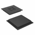 TMS320DM642AZDK6

The activity of extra discounts on wholesale prices is in full swing…
Please fill in your contact information and we will send you the latest wholesale price list.






