 ChipApex | Global Electronic Components Supplier

SEARCH
Search Product
Search Post
— IC芯片 | 连接器 | 传感器 | 被动器件 —
Search productSearch post
— IC芯片 | 连接器 | 传感器 | 被动器件 —
Consult the customer manager about the wholesale price.
consultation hotline:86-132-6715-2157
email:[email protected]
Contact the product manager for consultation. One-stop consultation is available.
Do you want a lower wholesale price? Please send us your inquiry and we will reply immediately.
TS4100ITQ1633T is listed in the Analog Switches - Special Purpose range at ChipApex. The manufacturer field lists Silicon Labs. Its product description is IC SWITCH 8:1 105 OHM 16QFN. Review the specifications below when checking this part for your BOM.
The TS4100ITQ1633T is an 8-channel analog multiplexer from the Silicon Labs TS410x family, housed in a 16-pin TQFN-16 (3.3 mm) package with an exposed paddle. It operates on a supply voltage range of 0.8 V to 5.25 V and supports input signal swings up to 5.25 V. The device features an on-resistance of 80 Ω typical at higher voltages, with less than 1% flatness variation across the entire signal swing. Supply current is 675 nA, and leakage currents are guaranteed below 0.5 nA. It functions within a temperature range of –40 °C to +85 °C.
Verify the ordering suffix 'T' indicates tape and reel packaging rather than tube. Confirm the specific part number matches the required 8-channel configuration. Ensure the design accommodates the exposed paddle for thermal management and electrical grounding as specified in the datasheet.
Select this component when low-voltage operation down to 0.8 V is required alongside high signal integrity. The Rail-to-Rail Plus feature is critical for applications where input signals must exceed the system supply voltage. Consider the 80 Ω on-resistance and 675 nA supply current for power-sensitive designs requiring precise analog switching.
This component belongs to the TS410x family, which includes the TS4101 dual 4-channel multiplexer and the TS4102 triple SPDT switch. All variants share the same 16-pin TQFN package and core technology but differ in channel count and topology. The TS4100 specifically provides a single 8:1 multiplexing path controlled by three address pins.
Public confirmed substitute part numbers are not available in the provided documentation.
The device utilizes "Rail-to-Rail Plus" technology, allowing input/output voltages to exceed the supply rails up to 5.25 V while maintaining a flat on-resistance.
In circuits with input/output impedances in the megaohm range, charge pump refreshes can generate transient spikes. Placing a 500 pF capacitor to ground at the input or output suppresses these spikes.
To prevent damage, the supply voltage should be applied first, followed by the voltage to the ADDA, ADDB, ADDC, and INH pins. If this sequence cannot be followed, a 500 kΩ resistor should be placed in series with the digital I/O pins.
Explore related parts through Interface, Integrated Circuits (ICs), all product categories, ChipApex homepage.
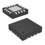 TS4100ITQ1633T

The activity of extra discounts on wholesale prices is in full swing…
Please fill in your contact information and we will send you the latest wholesale price list.





