 ChipApex | Global Electronic Components Supplier

SEARCH
Search Product
Search Post
— IC芯片 | 连接器 | 传感器 | 被动器件 —
Search productSearch post
— IC芯片 | 连接器 | 传感器 | 被动器件 —
Consult the customer manager about the wholesale price.
consultation hotline:86-132-6715-2157
email:[email protected]
Contact the product manager for consultation. One-stop consultation is available.
Do you want a lower wholesale price? Please send us your inquiry and we will reply immediately.
UJA1075TW/5V0/WD:1 is listed in the Specialized range at ChipApex. The manufacturer field lists NXP USA Inc.. Its product description is IC INTFACE SPECIALIZED 32HTSSOP. Review the specifications below when checking this part for your BOM.
The UJA1075TW/5V0/WD:1 is a high-speed CAN/LIN core System Basis Chip (SBC) designed for automotive Electronic Control Units (ECUs). It integrates a high-speed CAN transceiver compliant with ISO 11898-2 and ISO 11898-5, and a LIN transceiver compliant with LIN 2.1. The device features a scalable 5 V main voltage regulator (V1) delivering up to 250 mA for microcontroller supply, extendable via an external PNP transistor. A separate 5 V voltage regulator (V2) powers the on-board CAN transceiver. An advanced independent watchdog with Window and Timeout modes is included. Communication with the host microcontroller occurs via a full-duplex Serial Peripheral Interface (SPI). The component operates within a battery supply range of 4.5 V to 28 V and is housed in a 32-lead HTSSOP package.
Verify the specific ordering suffix against the manufacturer's official documentation to confirm regulatory compliance and feature set. Confirm that the package type matches the required thermal and physical constraints for the target application design.
Select this variant when a 5 V output is required for the microcontroller supply. Ensure the application utilizes the integrated watchdog functionality by verifying the WD suffix requirement. Compare against 3.3 V variants if lower voltage regulation is preferred for the host processor.
This component belongs to the NXP UJA1075 family of System Basis Chips. Variants within the family differ primarily in the output voltage of the main regulator (3.3 V vs. 5 V) and the inclusion of the watchdog timer. The TW designation indicates the specific HTSSOP32 package configuration.
Direct substitutes include other UJA1075 family members such as the UJA1075TW/3V3/WD:1 for 3.3 V applications. Verify pin compatibility and register mapping before replacing components with different voltage outputs or without the watchdog feature.
In Sleep mode, the CAN and LIN transceivers are switched off or enter a low-power state with bus wake-up detection active. The device remains capable of detecting wake-up events from the bus to transition back to Standby mode.
The LIMP pin serves as a limp home output. It is driven LOW to activate application-specific hardware in the event of a serious system malfunction or overtemperature condition.
Yes, the 250 mA main voltage regulator can be extended using an external PNP transistor. This allows for increased current capability and better heat distribution across the printed circuit board.
Explore related parts through Interface, Integrated Circuits (ICs), all product categories, ChipApex homepage.
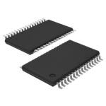 UJA1075TW/5V0/WD:1

The activity of extra discounts on wholesale prices is in full swing…
Please fill in your contact information and we will send you the latest wholesale price list.






