 ChipApex | Global Electronic Components Supplier
SEARCH
Search Product
Search Post
— IC芯片 | 连接器 | 传感器 | 被动器件 —
Search productSearch post
— IC芯片 | 连接器 | 传感器 | 被动器件 —
Consult the customer manager about the wholesale price.
consultation hotline:86-132-6715-2157
email:[email protected]
Contact the product manager for consultation. One-stop consultation is available.
Do you want a lower wholesale price? Please send us your inquiry and we will reply immediately.
The XC18V01PC20C0100 is a 3.3V in-system programmable configuration PROM from the XC18V00 series, designed for storing and reprogramming Xilinx FPGA configuration bitstreams. It features a 1-megabit (128K x 8) storage capacity and supports both serial and parallel interface modes for FPGA configuration. The device operates within an industrial temperature range of -40°C to +85°C and utilizes a low-power advanced CMOS FLASH process. It includes JTAG support for boundary-scan testing and in-system programming, ensuring data retention for a minimum of 20 years with an endurance of 20,000 program/erase cycles.
Verify component authenticity as this part is under obsolescence. Confirm the specific ordering suffix matches the required package type (PC20) and temperature grade. Ensure compatibility with existing FPGA designs regarding voltage levels and interface modes before procurement.
Select this device when a 1-megabit configuration memory is required for Xilinx FPGAs such as the XC2V80 or XCV100. Consider the PC20 package availability and verify that the system design supports either serial or parallel configuration modes. Evaluate the need for in-system programmability versus one-time programmable alternatives based on design flexibility requirements.
The XC18V01 is part of the XC18V00 series of 3.3V in-system programmable PROMs. This family includes variants with different capacities, such as the XC18V512, XC18V02, and XC18V04, to accommodate various FPGA configuration bitstream sizes. The series is characterized by its low-power CMOS FLASH technology and comprehensive JTAG support for manufacturing and field updates.
Public confirmed substitute part numbers are not available in the provided documentation due to the product's obsolete status. Designers should consult Xilinx application notes for recommended migration strategies or compatible legacy components.
In 20-pin packages, there is no dedicated CF pin. The CF function can be routed to pin 7 by setting the CF → D4 option, provided the parallel output mode is not used.
During power-up, the OE/RESET pin is held Low by the PROM to reset the address counter and keep outputs in a high-Z state until power supplies stabilize and reach POR thresholds.
Yes, the device supports in-system programming via JTAG using Xilinx iMPACT software or third-party JTAG development systems, and can also be programmed externally using a standard device programmer.
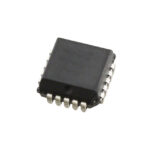 XC18V01PC20C0100
The activity of extra discounts on wholesale prices is in full swing…
Please fill in your contact information and we will send you the latest wholesale price list.





